Grolltex announces graphene plant expansion in San Diego to 30,000 eight Inch wafer equivalents

Graphene and 2D materials producer Grolltex has announced the completion of its recent capacity expansion and released production for 30,000 eight-inch wafer equivalents per year at its CVD monolayer fabrication facility in San Diego, California.

This is the only commercial CVD monolayer graphene production facility in California and in fact it is the largest capacity plant of its kind in the U.S., said CEO, Jeff Draa. Demand for our electronics grade graphene has never been better. Our production lines are capable of producing single layer graphene or single layer hexagonal Boron Nitride.
Read the full story Posted: Feb 27,2019

DTU team protects graphene with hBN for future electronics

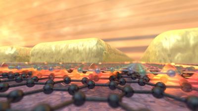
Graphene Flagship researchers at DTU, Denmark, solved the problem of graphene's accumulation of defects and impurities due to environmental exposure by protecting it with insulating layers of hexagonal boron nitride, another two-dimensional material with insulating properties.

DTU team protects graphene with hBN for future electronics image

Peter Bøggild, researcher at Graphene Flagship partner DTU and coauthor of the paper, explains that although 'graphene is a fantastic material that could play a crucial role in making new nano-sized electronics, it is still extremely difficult to control its electrical properties.' Since 2010, scientists at DTU have tried to tailor the electrical properties of graphene, by making a very fine pattern of holes, so that channels through which an electric power can flow freely are formed. 'Creating nanostructured graphene turned out to be amazingly difficult, since even small errors wash out all the properties we designed it to have,' comments Bøggild.

Read the full story Posted: Feb 20,2019

Korean researchers fabricate ordered graphene quantum dot arrays

A new study led by the Ulsan National Institute of Science and Technology in South Korea reveals a technology capable of fabricating highly ordered arrays of graphene quantum dots.

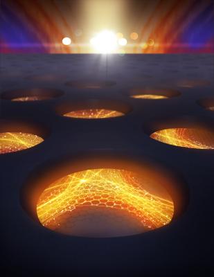
Korean researchers fabricate ordered graphene quantum dot arrays imageGraphene quantum dots of various sizes in a stable, ordered array

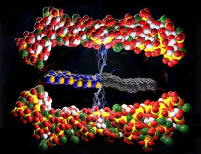
The research team demonstrated a novel way of synthesizing GQDs, embedded inside a hexagonal boron nitride (hBN) matrix. Thus, they demonstrated simultaneous use of in-plane and van der Waals heterostructures to build vertical single-electron tunneling transistors.

Read the full story Posted: Feb 10,2019

Graphene/hBN ceramic could act as a sensor for structures and aircraft

Rice University and Iran University of Science and Technology researchers have found a unique ceramic material that could act as a sensor for structures.

Graphene/hBN ceramic could act as a sensor for structures and aircraft image

The ceramic becomes more electrically conductive under elastic strain and less conductive under plastic strain, and could lead to a new generation of sensors embedded into structures like buildings, bridges and aircraft able to monitor their own health.

Read the full story Posted: Feb 06,2019

Graphene enables low-dimensional spintronics at room temperature

Graphene Flagship researchers produced graphene-based spintronics devices that utilize both electron charge and spin at room temperature. Demonstrating the spin’s feasibility for bridging distances of up to several micrometres, these results may open the door to new possibilities for integrating information-processing and storage in a single chip.

The Graphene Flagship program recognizes the potential of spintronics devices made from graphene-related materials. Researchers from different universities successfully showed that it is possible to manipulate graphene’s spin properties in a controlled manner at room temperature. These results inspire new directions in the development of spin-logic devices and quantum computing. With miniaturization a major driving force behind the electronics industry, graphene opens new possibilities for compacting spin-logic operations with magnetic memory elements in a single platform, notes Catalan Institution for Research and Advanced Studies (ICREA) Research Professor Stephan Roche, who has been leading the Graphene Flagships Spintronics Work Package since its inception.

Read the full story Posted: Jan 15,2019

Researchers design novel graphene-based terahertz detector

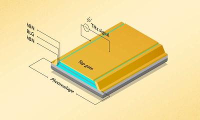
A team of researchers from Russia, UK, Japan and Italy has created a graphene-based terahertz detector.

Researchers design novel graphene-based terahertz detector image

The team explains that the reason for the inefficiency of existing terahertz detectors is the mismatch between the size of the detecting element, the transistor—about one-millionth of a meter—and the typical wavelength of terahertz radiation, which is about 100 times greater. This results in the wave passing the detector by without any interaction.

Read the full story Posted: Dec 23,2018

Researchers turn graphene into a molecular toggle switch

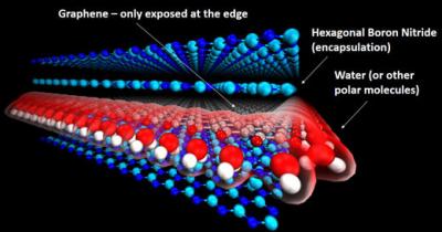
A team of researchers from Denmark, Italy and Portugal recently discovered a new mechanism for controlling electronic devices using molecules. The researchers have shown that the ferroelectric ordering of polar molecules attached to the edge of graphene can be toggle-switched by an electrostatic gate and can be used for memory devices and sensors.

turning graphene into a molecular toggle switch image

Molecular electronics aims to use individual molecules to control electronics. The large library of molecules and techniques to modify them can create more sophisticated electronics than previously thought possible. The normal hindrance is the small size of the molecules. It's possible to create them, but they are incredibly difficult to handle. It is almost impossible to manipulate small enough features in ordinary materials to electrically connect with individual molecules.

Read the full story Posted: Jul 29,2018

The dispute over the origins of terahertz photoresponse in graphene results in a draw

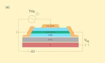
Researchers at the Russia-based MIPT, MSPU and the University of Manchester revealed the mechanisms leading to photocurrent in graphene under terahertz radiation. The paper is said to put an end to a long-lasting debate about the origins of direct current in graphene illuminated by high-frequency radiation, and also sets the stage for the development of high-sensitivity terahertz detectors. Such detectors have applications in medical diagnostics, wireless communications and security systems.

Wiring diagram of a graphene-based terahertz detector image

In 2005, MIPT alumni Andre Geim and Konstantin Novoselov experimentally studied the behavior of electrons in graphene and found that electrons in graphene respond to electromagnetic radiation with an energy of quantum, whereas the common semiconductors have an energy threshold below which the material does not respond to light at all. However, the direction of electron motion in graphene exposed to radiation has long remained a point of controversy, as there is an abundance of factors pulling it in different directions. The controversy was especially stark in the case of the photocurrent caused by terahertz radiation.

Read the full story Posted: Apr 26,2018

Flagship team uses graphene to squeeze light into one atom

Researchers at the Institute of Photonic Sciences (ICFO) in Spain, along with other members of the Graphene Flagship, have reached what they consider to be the ultimate level of light confinement - being able to confine light down to a space of one atom. This may pave the way to ultra-small optical switches, detectors and sensors.

Graphene Flagship team uses graphene to confine light to one atom image

Graphene keeps surprising us: nobody thought that confining light to the one-atom limit would be possible. It will open a completely new set of applications, such as optical communications and sensing at a scale below one nanometer, said ICREA Professor Frank Koppens at ICFO, who led the research.

Read the full story Posted: Apr 23,2018

Researchers design a method for detecting individual impurities in graphene

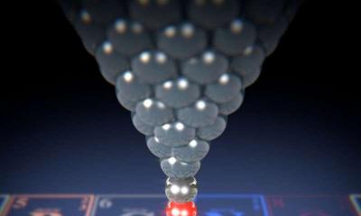
A team of researchers from the University of Basel, the National Institute for Material Science in Tsukuba in Japan, Kanazawa University, Kwansei Gakuin University in Japan and Aalto University in Finland has succeeded in using atomic force microscopy to obtain images of individual impurity atoms in graphene ribbons. Thanks to the forces measured in the graphene's two-dimensional carbon lattice, they were able to identify boron and nitrogen for the first time.

Researchers design a method to detect individual impurities in graphene image Using the atomic force microscope's carbon monoxide functionalized tip (red/silver), the forces between the tip and the various atoms in the graphene ribbon can be measured

The team replaced particular carbon atoms in the hexagonal lattice with boron and nitrogen atoms using surface chemistry, by placing suitable organic precursor compounds on a gold surface. Under heat exposure up to 400°C, tiny graphene ribbons formed on the gold surface from the precursors, including impurity atoms at specific sites.

Read the full story Posted: Apr 15,2018