Graphene Flagship welcomes sixteen new FLAG-ERA projects

The Graphene Flagship has announced 16 New FLAG-ERA projects, that cover a broad range of topics, from fundamental to applied research. These projects which will become Partnering Projects of the Graphene Flagship receiving around €11 million in funding overall.

Bringing together a diverse range of European knowledge and expertise, FLAG-ERA is an ERA-NET (European Research Area Network) initiative that aims to create synergies between new research projects and the Graphene Flagship and Human Brain Project.
Read the full story Posted: May 29,2020

MIT researchers use graphene and boron nitride to convert terahertz waves to usable energy

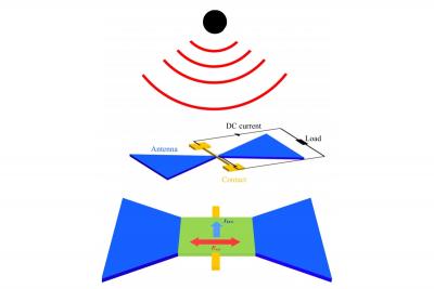
Researchers at MIT are working to develop a graphene-based device that may be able to convert ambient terahertz waves into a direct current. The MIT team explains that any device that sends out a Wi-Fi signal also emits terahertz waves —electromagnetic waves with a frequency somewhere between microwaves and infrared light. These high-frequency radiation waves, known as T-rays, are also produced by almost anything that registers a temperature, including our own bodies and the inanimate objects around us.

Graphene and boron nitride to help use terahertz energy image

Terahertz waves are pervasive in our daily lives, and if harnessed, their concentrated power could potentially serve as an alternate energy source. Imagine, for instance, a cellphone add-on that passively soaks up ambient T-rays and uses their energy to charge your phone. However, to date, terahertz waves are wasted energy, as there has been no practical way to capture and convert them into any usable form. This is exactly what the MIT scientists set out to do.

Read the full story Posted: Mar 30,2020

Graphene acts as superconductor, insulator and ferromagnet in a single device

A collaborative group of scientists has designed a device that makes use of graphene’s assorted talents: superconducting, insulating, and a type of magnetism called ferromagnetism. The multitasking device could enable new physics experiments, such as research in the pursuit of an electric circuit for faster, next-generation electronics like quantum computing technologies.

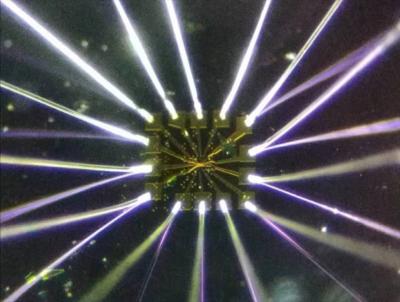
The graphene deviceon a silicon dioxide/silicon chip imageAn optical image of the graphene device (shown above as a square gold pad) on a silicon dioxide/silicon chip. Shining metal wires are connected to gold electrodes for electrical measurement. (Credit: Guorui Chen/Berkeley Lab)

So far, materials simultaneously showing superconducting, insulating, and magnetic properties have been very rare. And most people believed that it would be difficult to induce magnetism in graphene, because it’s typically not magnetic. Our graphene system is the first to combine all three properties in a single sample, said Guorui Chen, a postdoctoral researcher in Wang’s Ultrafast Nano-Optics Group at UC Berkeley, and the study’s lead author.

Read the full story Posted: Mar 05,2020

NIST-led team uses graphene to create and image coupled quantum dots

Researchers at the National Institute of Standards and Technology (NIST) and their colleagues have used graphene and STM technology to create and image a novel pair of quantum dots — tiny islands of confined electric charge that act like interacting artificial atoms. Such coupled quantum dots could serve as a robust quantum bit, or qubit, the fundamental unit of information for a quantum computer. Moreover, the patterns of electric charge in the island can’t be fully explained by current models of quantum physics, offering an opportunity to investigate rich new physical phenomena in materials.

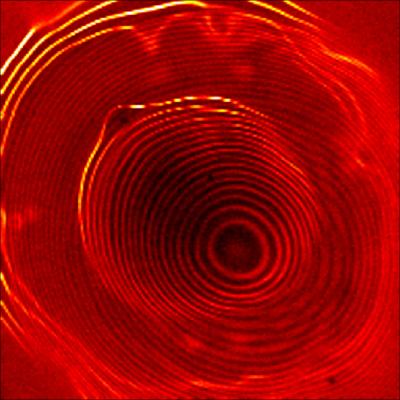
Graphene aids in imaging qubits imagea system of coupled quantum dots taken by STM shows electrons orbiting within two concentric sets of rings, separated by a gap. The inner set of rings represents one quantum dot; the outer, brighter set represents a larger, outer quantum dot. Credit: NIST

The NIST -led team included researchers from the University of Maryland NanoCenter and the National Institute for Materials Science in Japan. The team used the ultrasharp tip of a scanning tunneling microscope (STM) as if it were a stylus of sorts. Hovering the tip above an ultracold sheet of graphene, the researchers briefly increased the voltage of the tip.

Read the full story Posted: Jan 30,2020

Graphene enables researchers to visualize the flow of electrons

Researchers from Israel's Weizmann Institute and the UK's Manchester University have succeeded in imaging electrons' hydrodynamic flow pattern for the first time using a novel scanning probe technique. They have proven the longstanding scientific theory that electrons can behave like a viscous liquid as they travel through a conducting material, producing a spatial pattern that resembles water flowing through a pipe.

The results of this study could help developers of future electronic devices, especially those based on 2D materials like graphene in which electron hydrodynamics is important.

Read the full story Posted: Dec 12,2019

Stanford team finds novel form of magnetism in twisted bi-layer graphene

Stanford physicists recently observed a novel form of magnetism, predicted but never seen before, that is generated when two graphene sheets are carefully stacked and rotated to a special angle. The researchers suggest the magnetism, called orbital ferromagnetism, could prove useful for certain applications, such as quantum computing.

bi-layer graphene between hBN gives off orbital ferromagnetism imageOptical micrograph of the assembled stacked structure, which consists of two graphene sheets sandwiched between two protective layers made of hexagonal boron nitride. (Image: Aaron Sharpe)

We were not aiming for magnetism. We found what may be the most exciting thing in my career to date through partially targeted and partially accidental exploration, said study leader David Goldhaber-Gordon, a professor of physics at Stanford’s School of Humanities and Sciences. Our discovery shows that the most interesting things turn out to be surprises sometimes.

Read the full story Posted: Jul 28,2019

Graphene enables researchers to control infrared and terahertz waves

Researchers from the University of Geneva (UNIGE) in Switzerland and the University of Manchester in the UK have found an efficient way to control infrared and terahertz waves using graphene. "There exist a class of the so-called Dirac materials, where the electrons behave as if they do not have a mass, similar to light particles, the photons," explains Alexey Kuzmenko, a researcher at the Department of Quantum Matter Physics in UNIGE's Science Faculty, who co-conducted this research together with Ievgeniia Nedoliuk.

The interaction between graphene and light suggests that this material could be used to control infrared and terahertz waves. "That would be a huge step forward for optoelectronics, security, telecommunications and medical diagnostics," points out the Switzerland-based researcher.

Read the full story Posted: Jul 22,2019

Unique device that combines graphene and boron nitride can switch from superconducting to insulating

Researchers at the U.S. Department of Energy's Lawrence Berkeley National Laboratory (Berkeley Lab) have designed a graphene device that switches from a superconducting material to an insulator and back again to a superconductor — all with a flip of a switch. The team shared that the device exhibits this unique versatility while being thinner than a human hair.

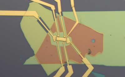
Graphene and hBN device moves from insulating to superconducting imageViews of the trilayer graphene/boron nitride heterostructure device as seen through an optical microscope. The gold, nanofabricated electric contacts are shown in yellow; the silicon dioxide/silicon substrate is shown in brown and the boron nitride flakes

"Usually, when someone wants to study how electrons interact with each other in a superconducting quantum phase versus an insulating phase, they would need to look at different materials. With our system, you can study both the superconductivity phase and the insulating phase in one place," said Guorui Chen, the study's lead author and a postdoctoral researcher in the lab of Feng Wang, who led the study. Wang, a faculty scientist in Berkeley Lab's Materials Sciences Division, is also a UC Berkeley physics professor.

Read the full story Posted: Jul 18,2019

Researchers develop washable, wearable graphene capacitors that can be woven directly into clothes

Researchers at the University of Cambridge and Jiangnan University in China have developed graphene-enhanced wearable electronic components incorporated directly into fabrics. The devices could be used for flexible circuits, healthcare monitoring, energy conversion, and other applications.

The researchers have shown how graphene and other related materials can be directly incorporated into fabrics to produce charge storage elements such as capacitors, paving the way to textile-based power supplies which are washable, flexible and comfortable to wear.

Read the full story Posted: May 16,2019

Graphene quantum dots to help create single electron transistors

Scientists from Manchester University, the Ulsan National Institute of Science & Technology and the Korea Institute of Science and Technology have developed a novel technology, which combines the fabrication procedures of planar and vertical heterostructures in order to assemble graphene-based single-electron transistors.

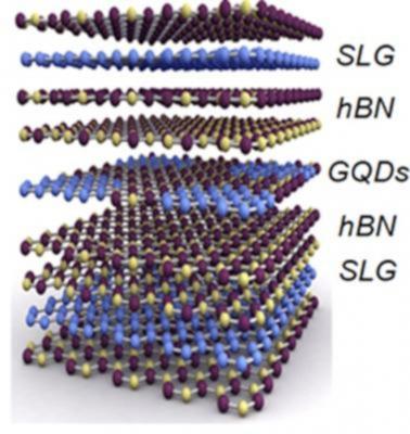
Graphene quantum dots to help create single electron transistorsThe schematic structure of the devices

In the study, it was demonstrated that high-quality graphene quantum dots (GQDs), regardless of whether they were ordered or randomly distributed, could be successfully synthesized in a matrix of monolayer hexagonal boron nitride (hBN). Here, the growth of GQDs within the layer of hBN was shown to be catalytically supported by the platinum (Pt) nanoparticles distributed in-between the hBN and supporting oxidised silicon (SiO2) wafer, when the whole structure was treated by the heat in the methane gas (CH4). It was also shown, that due to the same lattice structure (hexagonal) and small lattice mismatch (~1.5%) of graphene and hBN, graphene islands grow in the hBN with passivated edge states, thereby giving rise to the formation of defect-less quantum dots embedded in the hBN monolayer.

Read the full story Posted: Mar 08,2019