Graphene achieves superconductivity

A collaborative team from Tohoku University and the University of Tokyo has designed a way to make graphene superconductive, which means electrons can flow through it with zero resistance. This can lead to significantly more efficient electronic devices, power lines, high-speed electronic devices and more.

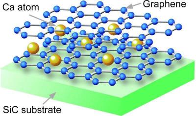
While exciting, it is important to say that this demonstration of superconductivity in graphene occurred at a temperature of -269 degrees Celsius, and room temperature superconductivity is still far from attainable. However, this research does suggest that graphene could be used to build nano-sized, high-speed electronic devices.

Read the full story Posted: Feb 17,2016

Will Samsung incorporate graphene electrodes in their upcoming OLED TVs?

The OLED Association, a trade group that promotes OLED technologies, published an interesting article in which they give predictions for the OLED market. The Association sees Samsung returning to the OLED TV market in 2017, and those upcoming OLED TVs will use several new technologies - including graphene-based transparent electrodes.

Last month we reported that researchers at Korea's ETRI developed transparent graphene-based electrodes for OLED panels. The researchers say that these new electrodes improve the transparency and "image quality" of OLEDs by 40 to 60 percent, compared to current silver-based electrodes. The researchers aim to continue the research and improve the performance of their electrodes.

Read the full story Posted: Jan 07,2016

Saint Jean Carbon to prototype graphene-based superconducting wire

Saint Jean Carbon, a publicly traded carbon science company, announced that it, along with their industry partners, will complete a prototype of a graphene-enhanced diamagnetic wire that will conduct energy at room temperature with superconducting level resistance. The process to build the wire is planned to take a few months, and the model will first be prototyped at 36 inches in length with a goal to measure the energy resistance under varying loads. This should, for example, give a better understanding on how a superconducting wire can greatly enhance the electricity transfer from an electric motor to a battery.

The design is based on relatively simple principles: the outer housing (casing) is a non-conductive rubber compound and the inner sleeve is a resin binder with a high concentration of diamagnetic graphene. The center core is a magnetic graphene wire and the diamagnetic force holds the center core in place while the energy passes along the path of the neutralized middle core.

Read the full story Posted: Dec 23,2015

Manipulating graphene's wrinkles could lead to graphene semiconductors

Researchers at Japan's RIKEN have discovered that wrinkles in graphene can restrict the motion of electrons to one dimension, forming a junction-like structure that changes from zero-gap conductor to semiconductor back to zero-gap conductor. Moreover, they have used the tip of a scanning tunneling microscope to manipulate the formation of wrinkles, opening the way to the construction of graphene semiconductors by manipulating the carbon structure itself in a form of "graphene engineering."

The scientists were able to image the tiny wrinkles using scanning tunneling microscopy, and discovered that there were band gap openings within them, indicating that the wrinkles could act as semiconductors. Two possibilities were Initially considered for the emergence of this band gap. One is that the mechanical strain could cause a magnetic phenomenon, but the scientists ruled this out, and concluded that the phenomenon was caused by the confinement of electrons in a single dimension due to "quantum confinement."

Read the full story Posted: Oct 26,2015

Will Stanene become graphene's rival in terms of electrical conductivity?

A collaboration between researchers at Stanford University and four universities in China yielded a material made of a single layer of tin atoms, that could be the world's first material to conduct electricity with 100% efficiency at room temperature. The material, called Stanene, is believed to be a rival to graphene and other two-dimensional materials like phosphorene, silicene or germanene, because it is believed to be so conductive as to allow flow of electricity without any heat loss.

The scientists created the mesh by vaporising tin in a vacuum and allowing the atoms to collect on a supporting surface of bismuth telluride. As a result, a two-dimensional honeycomb structure of tin atoms was made. Alas, the substrate and stanene interacted to disrupt the conditions that would have created the perfect conductor - so the team plans to use larger amounts of tin and an inert substrate to rule out interaction. In fact, not all researchers are even sure that the structure created at Stanford is indeed stanene. Direct measurements of the crystal arrangements only can confirm this but that will call for larger amounts of the material.

Read the full story Posted: Aug 05,2015

Unique process improves graphene's performance as a transparent conductor

Researchers from the University of Maryland found that intercalating (embedding) sodium ions in a reduced graphene oxide (rGO) network, printed with graphene oxide (GO) ink, can significantly improve its performance as a transparent conductor in displays, solar cells and electronic devices.

The scientists used cost-effective materials and production techniques to receive a highly scalable printed electronics system that produces relatively inexpensive and stable conductors. The team theorizes the increased stability is due to the natural oxidation of sodium along the edges of the printed networks which forms a barrier that prevents ion loss. Networks printed with the ink exhibit up to 79 percent optical transmittance and 311 Ohms per square of sheet resistance.

Read the full story Posted: Jun 08,2015

Cerious Technologies has graphene-based interconnects on the market

An American company called Cerious Technologies is now offering several types of graphene-based cables and interconnects for sale. Cerious is focused on manufacturing and selling audio products like speakers, sound systems and various audio cables and interconnects.

Cerious' Graphene Extreme is an interconnect cable that utilizes graphene (which Cerious states is of its own manufacture) as a conductor technology. The company says that the ultra fine conductor enables the cable to operate linearly well into the gigahertz while being non-magnetic. This eliminates ringing and the bounce that occurs from normal terminations. It offers deeper soundstage, more detail and quieter backgrounds.

Read the full story Posted: Jun 06,2015

FlexEnable details their graphene OTFT goals

UK-based FlexEnable was spun-off from Plastic Logic in February 2015 with an aim to further develop and commercialize the company’s technology platform for organic thin film transistor (OTFT) arrays for flexible displays and ubiquitous sensing. Last month FlexEnable joined the graphene flagship, and announced plans to develop new use cases for graphene in flexible electronics.

I talked briefly to Mike Banach, FlexEnable's Technical Director, and he explained the company's graphene plans and goals. FlexEnable is not a material company - they do not aim to develop and produce graphene material. The define themselves as a applied process technology - what we call a graphene application developer, focused on the flexible electronics market.

Read the full story Posted: May 17,2015

Plastic Logic and the CGC demonstrate the first graphene-based flexible display

In June 2013, Cambridge University's Graphene Centre (CGC) and Plastic Logic started to develop a transparent graphene-based backplane for flexible displays. Now Plastic Logic demonstrated the first display that was developed in that collaboration research. Plastic Logic says that this is the first time graphene has been used in a transistor-based flexible device.

The prototype (shown above) is an active-matrix electrophoretic (E Ink) display fabricated on flexible plastic. The electrodes are made from solution-processed graphene which was patterned after deposition with micron-scale features. The prototype has a pixel density of 150 PPI and was made at low temperatures (less than 100 degrees celsius). This is just a prototype of course and you can see many defects in display.

Read the full story Posted: Sep 07,2014