The University of Manchester installs a powerful high res microscope, will be used for graphene research

The University of Manchester have installed one of the world's most powerful high-res microscopes, the FEI Titan G2 80-200 scanning transmission electron microscope (S/TEM). The Titan G2 80-200 S/TEM will enable researchers to study the structure and elemental composition of materials at the atomic level.

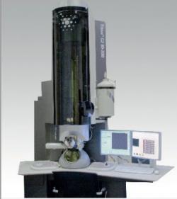
This new microscope may also help the University's graphene research - the Titan microscope's high-angle, dark-field imaging capability can potentially enable the discovery of new information about the electrical properties of graphene.

Read the full story Posted: Sep 04,2012

Osaka University bought an Aixtron BM Pro system to research graphene bio-sensors

Aixtron announced today that Osaka University in Japan placed an order for a 4" AIXTRON BM Pro system. The University will use the new equipment to produce carbon nanotube (CNT) and graphene structures for bio-sensors. The aim is to combine graphene field-effect transistors with organic chemicals, such as antibodies, antigens and aptamers to allow electrical detection of specific proteins. The BM Pro system will also be used to produce carbon nanotubes for micro-electromechanical-systems (MEMS) and energy storage devices.

Read the full story Posted: Sep 04,2012

Graphene Oxide may be toxic, kills bacteria

Some scientists are concerned that Graphene may be hazardous and toxic - for humans, animals and the natural environment. Researchers from Singapore's A*STAR have published a study on how graphite, graphite oxide, graphene oxide and reduced graphene oxide may effect bacteria (Escherichia coli in the study).

The researchers showed that the graphene-based materials kill substantially more bacteria than graphite-based materials. Graphene Oxide was the most dangerous material. The researchers say that most of the E.coli cells were individually wrapped by layers of graphene oxide. In contrast, E. coli cells were usually embedded in the larger reduced-graphene-oxide aggregates (see image above).

Read the full story Posted: Sep 02,2012

New technique creates thin, flexible and transparent graphene and boron-nitride films

Researchers from Cornell University have managed to pattern single atom films of graphene and boron nitride, an insulator, without the use of a silicon substrate. They are using a technique they call patterned regrowth, and they say this could lead towards substrate-free, atomically thin circuits. These will be so thin that they could be transparent and flexible, and yet have great electrical performance.

Patterned regrowth uses the same basic photolithography technology used in silicon wafer processing, and it allows graphene and boron nitride to grow in perfectly flat, structurally smooth films. The researchers first grew graphene on copper and used photolithography to expose graphene on selected areas, depending on the desired pattern. They filled that exposed copper surface with boron nitride, the insulator, which grows on copper and fills the gaps. Then you simply peel off the entire structure.

Read the full story Posted: Sep 02,2012

Researchers create the slimmest graphene nanoribbons ever

Researchers from IBM and University of California Riverside managed to make the slimmest graphene nanoribbon (GNR) ever - just 10 nm in width. Making one is virtually impossible, and the team created a large number of GNRs in parallel. The researchers say that the arrays cover about 50% of the prototype device channel area, which means that integrated circuits based on GNRs with the required high current densities are now possible. The narrow GNRs have a bandgap of about 0.2 eV.

The process the researchers used consists of two main steps: a top-down e-beam lithography step and a bottom-up self-assembly step involving a block copolymer template comprising alternating lamellae of the polymers PS and PMMA.

Read the full story Posted: Sep 02,2012