![]() IBM (NYSE: IBM) is a multinational technology and consulting corporation based in the US. IBM operates several research labs around the world and they are researching graphene related technologies - mostly graphene based transistors and photo detectors.
IBM (NYSE: IBM) is a multinational technology and consulting corporation based in the US. IBM operates several research labs around the world and they are researching graphene related technologies - mostly graphene based transistors and photo detectors.
In July 2014, IBM launched an ambitious 5-year $3 billion research initiative to find a silicon replacement for computer chips. Graphene is one of the materials under consideration.
1 New Orchard Road
Armonk, NY 10504-1722
United States
Graphene to enable tiny self-powered temperature sensors
A team of researchers from the University of Oxford, Delft University and IBM Zurich has demonstrated that graphene can be used to build sensitive and self-powering temperature sensors. The findings could pave the way for the design of highly sensitive thermocouples, which could be integrated in nanodevices and even living cells.
On-chip temperature sensors that are scalable, reliable and installable into nanodevices are essential for future thermal management in CPUs. By determining the local heating in certain segments of a CPU through the distribution of temperature monitors along critical points, feedback can be provided to a control system. In response, thermal management could allow for the redistribution of the thermal load through spot cooling or load distribution, for instance among different computing cores, avoiding hot spots and enabling a longer device lifetime as well as saving energy. Such temperature sensors should have a small footprint, high accuracy, consume a minimum amount of power and be compatible with established nanofabrication techniques.
IBM develops method to use graphene to deposit materials at a specific, nanoscale location
The Industrial Technology and Science group in IBM Research-Brazil, along with other academic collaboration partners, has reportedly proven for the first time that it is possible to electrify graphene so that it deposits material at any desired location at a solid surface with an almost-perfect turnout of 97%. Using graphene in this way enables the integration of nanomaterials at wafer scale and with nanometer precision.
 Artistic rendering of electric field-assisted placement of nanoscale materials between pairs of opposing graphene electrodes structured into a large graphene layer located on top of a solid substrate
Not only has this new work shown that it is possible to deposit material at a specific, nanoscale location, it was also reported that this can be done in parallel, at multiple deposition sites, meaning it’s possible to integrate nanomaterials at mass scale. This work has been patented.
IBM researchers use graphene to stimulate the body's immune response
IBM recently announced that its researchers have identified a new way to trigger the body's immune response by using polymer-coated graphene sheets.

In some medical treatments, it is crucial to target specific places in the body; To that end, scientists have developed techniques where drug molecules are attached directly to the surface of a nanomaterial, such as graphene sheets. Combining the nanomaterial and the drug molecules, these "nanotherapies" could help clinicians treat tumors, for example, by transporting the drugs directly to the tumors, where they can be released onto the cancer cells to help fight the disease.
Researchers manage to 'flatten' wrinkles in graphene
Scientists at MIT, along with researchers from IBM, the University of California at Los Angeles, and Kyungpook National University in South Korea, have found a way to produce graphene with fewer wrinkles, and to iron out the wrinkles that do appear. The team reports that the techniques successfully produce wafer-scale, "single-domain" graphene - single layers of graphene that are uniform in both atomic arrangement and electronic performance.
After fabricating and then flattening out the graphene, the researchers tested its electrical conductivity. They found each wafer exhibited uniform performance, meaning that electrons flowed freely across each wafer, at similar speeds, even across previously wrinkled regions.
IBM swaps silicon for carbon nanotubes in transistors
![]() IBM scientists announced a remarkable engineering achievement - they have managed to exchange the silicon transistor contacts in transistors for smaller, more efficient, carbon nanotubes. This could have revolutionary potential as silicon is getting harder to shrink in size, while CNTs can allow a reduction in the size of transistors.
IBM scientists announced a remarkable engineering achievement - they have managed to exchange the silicon transistor contacts in transistors for smaller, more efficient, carbon nanotubes. This could have revolutionary potential as silicon is getting harder to shrink in size, while CNTs can allow a reduction in the size of transistors.
The smaller silicon transistor contacts get, the higher their electrical resistance becomes. There comes a point where the components simply get too small to conduct electrons efficiently and it seems that silicon is nearing that point. Carbon nanotubes, on the other hand, are a different story. They measure less than 10 nanometers in diameter (less than half the size of today's smallest silicon transistor contact) and IBM actually had to devise a new means of attaching these tiny components. Known as an "end-bonded contact scheme" the 10 nm electrical leads are chemically bonded to the metal substructure. Replacing these contacts with carbon nanotubes won't just allow for computers to crunch more data, faster. This breakthrough ensures that they'll continue to shrink, following Moore's Law, for several iterations beyond what silicon components are capable of.
IBM issues patent for a graphene-based identification system
![]() Recent reports indicate the issue of a patent assigned to IBM, regarding a graphene resistor based tamper resistant identifier with contactless reading. The invention seems to relate to an identification system that is more immune to copying than traditional barcodes.
Recent reports indicate the issue of a patent assigned to IBM, regarding a graphene resistor based tamper resistant identifier with contactless reading. The invention seems to relate to an identification system that is more immune to copying than traditional barcodes.
The method for creating this invention includes arranging an array of graphene resistors in parallel or series. The method also includes forming a unique identification code based on respective temperatures emanating from respective voltages output from the graphene resistors when the array of graphene resistors is in a powered state. Another aspect described in the patent application is an authentication apparatus that includes a plurality of graphene resistors with a bandgap voltage generation circuit or a bandgap current generation circuit connected to the plurality of graphene resistors for powering up the plurality of graphene resistors in the powered state.
IBM suggests using graphene as a reusable substrate for semiconductor growth
IBM developed a new method to use graphene as a substrate for single-crystalline semiconductor film growth. Graphene will be less expensive than current single-crystalline wafers used in such production methods, as it can be reused indefinitely.
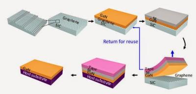
IBM says that growing a 4" GaN film today requires a 4" SiC substrate wafer which is destroyed using the process. The SiC costs about $3,000. Graphene can be used to replace the SiC and will be much cheaper in the long run. Graphene is also useful as it is flexible and can be better adapted for films that need to be transferred to a flexible substrate.
A new method produces well-defined high-quality nano graphene flakes
Researchers from Spain's University of Santiago de Compostela and IBM developed an extremely simple method to make high-quality well-defined nano graphene flakes from perylene, a common organic compound.
The new method uses arynes as molecular glue to paste graphene fragments together. This results in "clover-shaped" graphene flakes that are deposited on thin insulating films. It is possible to create those nano flakes in different sizes and shapes.
IBM to invest $3 billion trying to seek the next-gen chip technology, graphene is a candidate
IBM is an embarking on an ambitious project to find the next-generation chip technology to replace silicon. IBM will invest $3 billion over the next five years in this project. IBM will look into graphene, carbon nanotubes, quantum computing, silicon photonics and more technologies.
 GFET radio frequency receiver IC (IBM)
In the first stage of the project, they will try to build transistors in a 7 nm process, which they believe is already possible using silicon technology available today. But the second stage will look into different materials and architectures. IBM says that it is getting more and more difficult to shrink silicon chips further and silicon is reaching its limits.
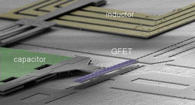
IBM researchers fabricated the world's most advanced G-FET based IC
IBM researchers built a graphene (GFET) based radio frequency receiver IC which they say is the world's most advanced IC ever made of graphene - in fact it offers 10,000 times better performance and any previously reported effort.
IBM's circuit consists of three graphene transistors, four inductors, two capacitors, and two resistors. All circuit components are fully integrated into a 0.6 mm2 area and fabricated in a 200 mm silicon production line. The researchers say that those the circuits consume less than 20 mW power to operate, while also demonstrating the highest conversion gain of any graphene RF circuits at multiple GHz frequency.