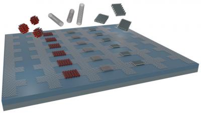
The Industrial Technology and Science group in IBM Research-Brazil, along with other academic collaboration partners, has reportedly proven for the first time that it is possible to electrify graphene so that it deposits material at any desired location at a solid surface with an almost-perfect turnout of 97%. Using graphene in this way enables the integration of nanomaterials at wafer scale and with nanometer precision.
 Artistic rendering of electric field-assisted placement of nanoscale materials between pairs of opposing graphene electrodes structured into a large graphene layer located on top of a solid substrate
Not only has this new work shown that it is possible to deposit material at a specific, nanoscale location, it was also reported that this can be done in parallel, at multiple deposition sites, meaning it’s possible to integrate nanomaterials at mass scale. This work has been patented.
Graphene is the thinnest material capable of conducting electricity and propagating electric fields. The electric fields are what scientists use to place nanomaterials on a graphene sheet: the shape and pattern of the graphene determines where the nanomaterials are placed. This offers an unprecedented level of precision for building nanomaterials. Today, this approach is done using standard materials, mostly metals such as copper. But the challenge arises from the fact that it is nearly impossible to remove the copper from the nanomaterials once it’s been assembled, without impacting the performance or destroying the nanomaterial completely. Graphene not only enables precision in placement of nanomaterials, but is easily removable from the assembled nanomaterial.
The IBM team stated that the method works regardless of the nanomaterial’s shape, for example, with quantum dots, nanotubes, and two-dimensional nanosheets. The researchers have used the method to build functioning transistors and to test their performance. In addition to integrated electronics, the method may be utilized for particle manipulation and trapping in lab-on-chip (microfluidics) technology.
The advancement in using graphene for nanomaterial placement could be used to create next-generation solar panels, faster chips in cell phones and tablets, or exploratory quantum devices, like an electrically controlled, on-chip quantum light emitter or detector. Such a device is able to emit or detect single photons, a prerequisite for secure communication.
This latest research suggests that graphene could enable the integration of nanomaterials that standard materials (used today) are not able to do. This could pave the way for its inclusion into industrial-scale electronics manufacturing. By working with industrial partners, IBM hopes to accelerate the knowledge generation, technology development and adoption of this bottom-up method for integration of nanomaterials.