IBM developed a new method to use graphene as a substrate for single-crystalline semiconductor film growth. Graphene will be less expensive than current single-crystalline wafers used in such production methods, as it can be reused indefinitely.
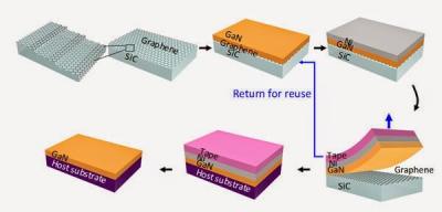
IBM says that growing a 4" GaN film today requires a 4" SiC substrate wafer which is destroyed using the process. The SiC costs about $3,000. Graphene can be used to replace the SiC and will be much cheaper in the long run. Graphene is also useful as it is flexible and can be better adapted for films that need to be transferred to a flexible substrate.
IBM has been researching graphene for a long time. A coupe of months ago, the company announced an ambitious project to find the next-generation chip technology to replace silicon. IBM will invest $3 billion over the next five years in this project, which will look at several alternatives including graphene.

