Researchers from Cornell University have managed to pattern single atom films of graphene and boron nitride, an insulator, without the use of a silicon substrate. They are using a technique they call patterned regrowth, and they say this could lead towards substrate-free, atomically thin circuits. These will be so thin that they could be transparent and flexible, and yet have great electrical performance.
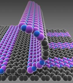
Patterned regrowth uses the same basic photolithography technology used in silicon wafer processing, and it allows graphene and boron nitride to grow in perfectly flat, structurally smooth films. The researchers first grew graphene on copper and used photolithography to expose graphene on selected areas, depending on the desired pattern. They filled that exposed copper surface with boron nitride, the insulator, which grows on copper and fills the gaps. Then you simply peel off the entire structure.