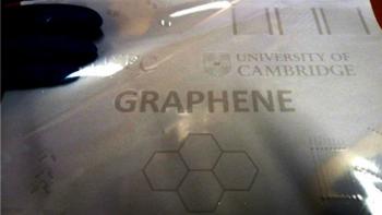
The Cambridge Graphene Centre deployed a new Agilent AFM microscope

The Cambridge Graphene Centre deployed a new scanning microscope to support their 2D material research. CGC installed an Agilent Technologies 5600LS atomic force microscope.

Agilent's AFM supports up to 300x300 mm samples and multi-sample 2-inch-wafers. It can be used with liquid samples and Agilent says it's got an exclusive SMM mode that offers calibrated electrical measurement capabilities.

Read the full story Posted: Jan 25,2014

Phosphorene, a new 2D material is a native p-type semiconductor

Researchers from Purdue University developed a new graphene-like 2D material from phosphorus. They call the new material phosphorene and they say that this is the first native 2D p-type semiconductor, making it more useful than graphene to make transistors.

Together with MoS2 (a 2D n-type semiconductor), it is now possible to build switches made from 2D materials. Graphene in its basic form is a superconductor and so is less suited to make transistors.

Read the full story Posted: Jan 24,2014

Students use pencil and paper to create strain and chemical sensors

Students from Northwestern University managed to use pencils and regular paper to create functional sensor devices. They created two types of sensors - strain sensors and chemical vapor sensors.

Pencil and paper strain sensor

The students had a discussion about the conductive properties of graphene. They realized that when you draw a line on a piece of paper with a pencil, the pencil's graphite sheds numerous graphene sheets. They started exploring what these graphene sheets can be used for, and the first thing they tried is making a basic electrode.

Read the full story Posted: Jan 24,2014

Graphenea slashes its graphene prices by 27% thanks to increased production efficiency and process yields

last month Graphenea announced that it has received a €1 million ($1.36 million) investment which will be used to accelerate Graphenea's business plan towards industrialization. Today the company announced it reduced prices by around 27% due to increased production efficiency, an improvement in process yield, and the acquisition of new lab equipment.

The company also announced that in 2014 it will invest in improved quality control equipment and processes to ensure that they will be able to offer high batch-to-batch reproducibility. They also said they expect the price of graphene to continue to decrease in coming years. Graphenea's current pilot graphene production line has an annual capacity of 150,000 square centimeters per year.

Read the full story Posted: Jan 22,2014

A new European project to develop ALD-processing of graphene

The European Union launched a new project called QUNTIHEAT (QUANTItative scanning probe microscopy techniques for HEAT transfer management in nanomaterials and nanodevices), and as part of that project the project partners will develop ALD-processing of graphene.

Picosun Oy, an ALD technology provider is part of that project. The company says that they will utilize their current ALD know how to enable ALD deposition of graphene. They hope this new deposition technology may be applied to produce displays, flexible electronics and components base don graphene.

Read the full story Posted: Jan 22,2014

Graphene 3D labs filed a provisional patent for graphene-enhanced 3D printing materials

Two months ago, Graphene Labs and Lomiko Metals launched a new company called Graphene 3D Labs that focuses on the development of high-performance graphene-enhanced materials for 3D Printing. Now we hear that Graphene 3D Lab filed a provisional patent application for the use of graphene-enhanced material, along with other materials, in 3D printing. This will enable the 3D printing of electronics devices - such as electronic circuits, sensors, or batteries.

The company's CEO, Daniel Stolyarov, says that they use Lomiko's high-quality graphene as the base material for producing graphene nanoplatelets, due to their cost and consistency in quality. The company says that adding graphene to polymers which are conventionally used in 3D printing improves the properties of the polymer in many different ways; it improves the polymers mechanical strength as well as its electrical and thermal conductivity.

Read the full story Posted: Jan 21,2014

BASF and the National University of Singapore to jointly develop graphene for OLEDs and OPVs

BASF logoThe Graphene Research Centre (GRC) at the National University of Singapore (NUS) and BASF announced a new partnership to develop the use of graphene in organic electronics devices - such as OLED devices. The goal of this collaboration is to interface graphene films with organic electronic materials, with an aim to create more efficient and flexible lighting devices.

In this collaboration, the GRC will contribute its graphene knowledge (the synthesis and characterization of the graphene) while BASF is focused on organic materials. Of course BASF is also engaged with graphene research (for several years) and are looking to speed up their device development with this new partnership.

Read the full story Posted: Jan 20,2014

Korean researchers develop a new method to synthesize large area MoS2 sheets

Researchers from Korea's Institute for Basic Science (IBS) developed a new way to synthesize single-layer molybdenum disulphide (MoS2) using a gold catalyst. This new method allows MoS2 to be synthesized within a large area and any desired geometrical shape, and to be produced in the form of a semiconductor device.

The researched used the principle that a surface alloy is formed through the separation of molybdenum atoms and mixing them with gold when a chemical compound containing molybdenum is injected onto the surface of gold.

Read the full story Posted: Jan 17,2014

Graphene Oxide is an efficient skin cancer photothermal therapy material

Researchers from Korea developed a new skin cancer photothermal therapy using graphene oxide. The idea is to attach the GO particles to tumor cells, and then shine near-infrared laser light on them. The GO generate heat (and destroy the tumor cells) when exposed to the light, while healthy cells are not effected. Graphene is more efficient than gold for converting the light into heat, and it's also cheaper.

The researcher coupled the graphene with hyaluronic acid, a sugar polymer that is found naturally in skin and is an ingredient in skin care products. The polymer can penetrate the skin’s top layer, and tumor cells are known to express a large number of hyaluronic acid receptors on their surfaces. So this coupling allows the researchers to apply the graphene oxide particles to the skin, avoiding the need to inject them.

Read the full story Posted: Jan 17,2014

Perovskite and graphene enable cheap and efficient solar cells

European researchers developed, produced and characterized a photovoltaic device based on a combination of titanium oxide and graphene as charge collector and Perovskite as sunlight absorber. This PV cell can be produced at low temperatures and is very efficient at 15.6% - higher than graphene combined with silicon.

Perovskite structures absorb sunlight very effectively, and this new development is a milestone for the progress of perovskite solar cells.

Read the full story Posted: Jan 15,2014