Graphenea demonstrated how gallium nitride (GaN) can be grown on silicon using graphene as an intermediary layer. GaN (and other semiconductors) are very appealing for applications such as LEDs, lasers and high-frequency and high-power transistors, and silicon is a great substrate for this, but it is very difficult to grown high-quality epitaxial GaN films on Si(100).
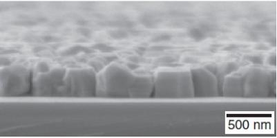
Graphene (in collaboration with MIT,Ritsumeikan University, Seoul National University and Dongguk University) found out that graphene can be used as an intermediary layer in such a structure. The hexagonal lattice of graphene has the same symmetry as that of GaN, and it can also be easily transferred to a silicon wafer. The company's method results in the best GaN(0001) layers on Si(100) demonstrated to date.
Graphene starts with a CVD-grown graphene on copper, which is then transferred to a silicon substrate and the copper is etched away. GaN is then grown directly on the graphene using radio-frequency molecular beam epitaxy (RF-MBE).