Researchers at Aalto University in Finland have fabricated an electricity-conducting material with promising properties by merging graphene and another 2D material, gallium selenide. The newly designed heterojunction could prove important for applications like sensors and wearable electronics and are, in comparison similar components that contain silicon, extremely thin. They also have impressive properties and the method used for their preparation is simpler than previous researched methods.
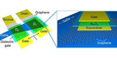
The component structure utilized elements from both lateral and vertical device design enabling the use of standard fabrication methods utilized in the semiconductor industry instead of laborious manual fabrication. The scientists explain that their inspiration comes from the existing silicon technology, aiming to bring out the state-of-the-art fabrication of 2D material devices from research labs to industry. In addition to the new and simpler way of manufacturing, the components have excellent characteristics like the on/off ratio, which is a critical parameter in electronics - over 10³.

