Chlorine doping proves a good way to open a band gap in graphene without harming the electronic properties

Researchers from MIT developed a new way to p-dope graphene (and open up a bandgap) without harming the material's electronic properties a lot. The process basically dopes with chlorine using a plasma-based surface functionalization technique. The researcher say that their chlorine-doped graphene keeps a high charge mobility (around 1500 cm2/V) after the hole doping.

Using this process, you can get the chlorine to cover over 45% of the graphene surface, the highest surface coverage area reported for any graphene doping material. In theory, covering 50% of the graphene with chlroine in both sides can open up a 1.2 eV band gap. This means that the 45% currently achieved is very close to this target. The researchers plan to start using suspended graphene sheets so that they can cover both sides.

Read the full story Posted: Aug 28,2013

The Wall Street Journal reports on the graphene IP gold rush

The wall street journal posted an interesting article and video on graphene. The article discusses the current state of research and business, possible graphene applications and the rush to patent related technologies.

The article starts with the Cambridge graphene research center and then discusses several companies and their graphene programs, including IBM, Nokia, BlueStone Global Tech, Vorbeck Materials, Lockheed Martin and Aixtron.

Read the full story Posted: Aug 26,2013

Graphene's negative resistance may enable ultra-fast, small circuits

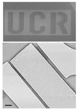
Researchers from the University of California, Riverside developed a graphene based transistor based on negative resistance rather than trying to open up a band gap. Negative resistance is the counterintuitive phenomenon in which a current entering a material causes the voltage across it to drop. It was shown before that graphene demonstrates negative resistance in certain circumstances.

The idea is to take a regular graphene field-effect transistor (FET) and find the circumstances in which it demonstrates negative resistance. This dip in voltage is used as a kind of switch - to perform logic. The researchers showed how several graphene FETs combined can be manipulated to produce conventional logic gates. The researchers designed such circuits that can match patterns (but they have yet to actually produce them).

Read the full story Posted: Aug 21,2013

Tiny twists in bilayer graphene ruin the material's theoretical bandgap

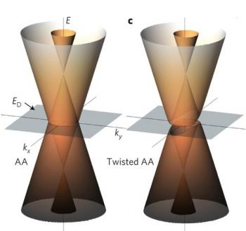
Bilayer graphene is supposed to have a bandgap, but experiments showed that this material cannot be turned into a real insulator. Now researchers from Berkeley Lab's Advanced Light Source (ALS) institute discovered that this is caused by tiny twists in the bilayer material, caused by subtle misalignments of the two layers. This twist can lead to surprisingly strong changes in the bilayer graphene's electronic properties.

The graphene layers twist produces massive and massless Dirac fermions. This structure prevents bilayer graphene from becoming fully insulating even under a very strong electric field. The researchers explain that Massless Dirac fermions are essentially electrons that act as if they were photons. As a result, they are not restricted by the same band gap constraints as conventional electrons. These new massless Dirac fermions move in a completely unexpected way governed by the symmetry twisted layers.

Read the full story Posted: Aug 16,2013

Bilayer graphene solitons act like electrical highways

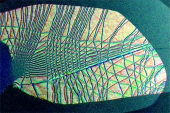
Researchers from Cornell University have shown that in bilayer graphene, defects can influence the conductivity. In fact, the bilayer graphene, when it is stacked and staggered, has ripples (called solitons) which act like electrical highways. The rest of the non-rippled bi-layer graphene is semiconducting.

Up until now it was predicted that bilayer graphene is uniformly semiconducting when stacked and staggered. The researchers say that ideally they'd like to get rid of those solitrons, or control their formation - to have one "electrical highway" but not so many. So controlling bilayer graphene solitrons may enable controlling graphene's electrical properties.

Read the full story Posted: Jul 12,2013

Haydale announce HDPlas graphene-based inks

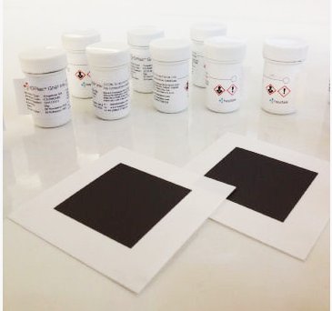
Haydale announced that it has developed new metal-free graphene-based inks. The HDPlas Graphene Ink Sc213 can be used to commercialize smart packaging, printed batteries, sensors, flexible displays (OLEDs and e-paper) and touch screens.

Haydale developed the new inks in collaboration with specialist ink manufacturer Gwent Electronic Materials (GEM). Those inks have been optimized for ideal viscosity and solid contents ensuring excellent coverage and exceptional conductivity. The inks are fully customisable and can be modified with development partners for specific requirements.

Read the full story Posted: Jun 26,2013

US Researchers find a method to control the growth of uniform atomic layers of molybdenum disulfide

Researchers from Rice University and the Oak Ridge National Laboratory (ORNL) found a new method to control the growth of uniform atomic layers of molybdenum disulfide (MDS), a semiconductor together with graphene can be used to make 2D electronic devices. Unlike graphene, MDS has a band gap.

The researchers goal is to create large MDS sheets (using CVD) and then use it together with graphene and the insulator hexagonal boron nitride (hBN) to form field-effect transistors, integrated logic circuits, photodetectors and flexible optoelectronics. MD5 isn't flat - it's actually a stack, with a layer of molybdenum atoms between two layers of sulfur atoms. It's a challenge to actually bind these three materials together.

Read the full story Posted: Jun 12,2013

Graphene and Molybdenite based flash memory is efficient, flexible, small and fast

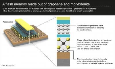
Researchers from EPFL designed a new flash memory cell prototype that is made from graphene and Molybdenite (MoS2). They say that the new design is efficient, flexible, small and fast. The idea is that the unique electronic properties of MoS2 (it has an "ideal energy band") are combined with graphene's excellent conductivity.

The EPFL design uses field-effect geometry. A thin layer of MoS2 is in the middle layer that channels electrons. The electrodes on the top and the bottom are made from graphene.

Read the full story Posted: Mar 20,2013

A bandgap can be opened in graphene using CH-Pi interactions

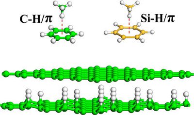
According to a theoretical study, opening a band gap in graphene can be practically opened by using CH-Pi interactions. The researchers from the Department of Chemistry at the University of Puerto Rico say that due to the equivalence breaking of two sublattices of graphene, a 90 meV band gap is opened in graphene/C4H bilayer. The band gap can be further increased to 270 meV by sandwiching graphene between two C4H layers.

This is the first time the CH/Pi interaction (a weak hydrogen-bond occurring between soft acids and soft bases) in graphene has been studied.

Read the full story Posted: Feb 03,2013

New method to make ordered GO with good electronic properties

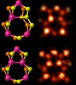
Unlike graphene, graphene-oxide (GO) has a bandgap, but has poor electronic properties (due to disorganized arrangement of atoms). Now researchers from the University of Wisconsin—Milwaukee have developed a method to make ordered GO. They hope that this method will enable "ideal bandgap" carbon based devices to be used as transistors, sensors and optoelectronic devices.

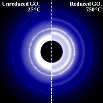
The researchers made a device made from layers of oxygen-poor graphene sandwiched between layers of GO, and then annealed (heated) it. The resulting device (shown on the right of the image above) has a more complex and ordered structure (you can see this as the extra rings in the image).

Read the full story Posted: Nov 28,2012