Electronics

Researchers develop a scalable method to reduce the contact resistance of graphene

The exceptional electronic properties of graphene make it a material with large potential for low-power, high-frequency electronics. However, the performance of a graphene-based device depends not only on the properties of the graphene itself, but also on the quality of its metal contacts. The lack of effective and manufacturable approaches to establish good ohmic contacts to a graphene sheet is one of the factors that currently limit the full application potential of graphene technology. The quality of the graphene-metal contacts is described in terms of the contact resistance (RC). Low RC values are crucial for any high-frequency or low-power application. Graphene’s low density of states near the charge neutrality point (Dirac point) limits carrier injection from metals, often resulting in high RC values.

(a–d) Schematics showing the process sequence for manufacturing the devices and the laser irradiation of graphene in the contact regions. (e) Optical micrograph of one of the measured devices. Image credit: AMO

Recently, researchers from RWTH Aachen University and AMO have developed a scalable method based on laser irradiation of graphene to reduce the RC in nickel-contacted devices. A laser with a wavelength of l = 532 nm is used to induce defects at the contact regions, which are monitored in situ using micro-Raman spectroscopy. 

Read the full story Posted: Jul 11,2024

Researchers develop a 2D device for quantum cooling

Researchers at École Polytechnique Fédérale de Lausanne (EPFL) in Switzerland and National Institute for Materials Science in Japan have combined the electrical properties of graphene with the semiconducting characteristics of indium selenide in a field-effect geometry, to create a device that can efficiently convert heat into electrical voltage at temperatures lower than that of outer space. The innovation could help overcome a significant obstacle to the advancement of quantum computing technologies, which require extremely low temperatures to function optimally.

Device schematic representing a fully encapsulated few-layer InSe channel, with graphene electrodes. Image credit: Nature Nanotechnology

To perform quantum computations, quantum bits (qubits) must be cooled down to temperatures in the millikelvin range (close to -273 Celsius), to slow down atomic motion and minimize noise. However, the electronics used to manage these quantum circuits generate heat, which is difficult to remove at such low temperatures. Most current technologies must therefore separate quantum circuits from their electronic components, causing noise and inefficiencies that hinder the realization of larger quantum systems beyond the lab. Now, researchers in EPFL’s Laboratory of Nanoscale Electronics and Structures (LANES), led by Andras Kis, have fabricated a device that not only operates at extremely low temperatures, but does so with efficiency comparable to current technologies at room temperature.

Read the full story Posted: Jul 06,2024

Researchers show that trilayer graphene with a twist could speed up electrochemical reactions

Researchers from the University of Michigan, SLAC National Accelerator Laboratory, Carnegie Mellon University and Harvard University have shown that three layers of graphene, in a twisted stack, benefit from a similar high conductivity to "magic angle" bilayer graphene but with easier manufacturing—and faster electron transfer. The findings could improve nano electrochemical devices or electrocatalysts to advance energy storage or conversion.

Twisting two sheets of graphene at a 1.1° angle, dubbed the "magic angle," creates a "flat band" structure, meaning the electrons across a range of momentum values all have roughly the same energy. Because of this, there is a huge peak in the density of states, or the available energy levels for electrons to occupy, at the energy level of the flat band which enhances electrical conductivity. Recent work experimentally confirmed these flat bands can be harnessed to increase the charge transfer reactivity of twisted bilayer graphene when paired with an appropriate redox couple—a paired set of chemicals often used in energy storage to shuttle electrons between battery electrodes. Adding an additional layer of graphene to make twisted trilayer graphene yielded a faster electron transfer compared to bilayer graphene, according to the team's recent study, that created an electrochemical activity model.

Read the full story Posted: Jun 26,2024

Black Semiconductor secures €254.4 million in funding

German semiconductor startup, Black Semiconductor, has secured EUR 254.4 million (around USD$275,900,000) in funding to launch graphene-enhanced semiconductor technology in Europe. With the funding, the company says that it is on track to realize the first phase of its vision – advancing a new generation of chip technology from research to mass production by 2031.

The Company has secured EUR 228.7 million (around USD$248,000,000) in public funding from the German Ministry of Economic Affairs and Climate Action and the state of North Rhine-Westphalia over the next 7 years under the IPCEI ME/CT2 program.

Read the full story Posted: Jun 12,2024

Researchers report quantum anomalous Hall effect in rhombohedral graphene

Researchers at the Massachusetts Institute of Technology (MIT), University of Texas at Dallas and Japan's National Institute for Materials Science have reported the quantum anomalous Hall effect (QAHE), a topological phenomenon that features quantized Hall resistance at zero magnetic field, in a rhombohedral pentalayer graphene-monolayer tungsten disulfide (WS2) heterostructure. 

This achievement can also be described as a 'five-lane superhighway' for electrons, that could allow ultra-efficient electronics and more. The team explained that its discovery could have direct implications for low-power electronic devices because no energy is lost during the propagation of electrons, which is not the case in regular materials where the electrons are scattered.

Read the full story Posted: May 14,2024

Researchers grow graphene nanoribbons in hBN stacks

Van der Waals encapsulation of 2D materials in hBN stacks could be a promising way to create ultrahigh-performance electronic devices. However, current approaches for achieving van der Waals encapsulation, which involve artificial layer stacking using mechanical transfer techniques, are difficult to control, prone to contamination and unscalable. 

Researchers at Shanghai Jiao Tong University, Wuhan University, Ulsan National Institute of Science and Technology, National Institute for Materials Science and Tel Aviv University recently reported the transfer-free direct growth of high-quality graphene nanoribbons (GNRs) in hexagonal boron nitride (hBN) stacks. The as-grown embedded GNRs exhibited highly desirable features being ultralong (up to 0.25 mm), ultranarrow (<5 nm) and homochiral with zigzag edges. 

Read the full story Posted: May 03,2024

Researchers electrically manipulate a ‘chiral interface state’ in a 2D material

Researchers from  Purdue University, University of California, Lawrence Berkeley National Laboratory and Japan's National Institute for Materials Science have managed to electrically manipulate a ‘chiral interface state’ in twisted monolayer-bilayer graphene, with potential for energy-efficient microelectronics and quantum computing.

The international research team, led by Lawrence Berkeley National Laboratory (Berkeley Lab), has taken the first atomic-resolution images and demonstrated electrical control of a chiral interface state – an exotic quantum phenomenon that could help researchers advance quantum computing and energy-efficient electronics.

Read the full story Posted: Apr 11,2024

Researchers use graphene to develop protective layer for 2D quantum materials

Researchers at the Würzburg-Dresden Cluster of Excellence ct.qmat, along with additional collaborators, have developed a graphene-based protective film that shields quantum semiconductor layers just one atom thick from environmental influences without compromising their quantum properties. This could advance the use of these delicate atomic layers in ultrathin electronic components.

A few years ago, scientists from the Cluster of Excellence ct.qmat discovered that topological quantum materials such as indenene hold great promise for ultrafast, energy-efficient electronics. These extremely thin quantum semiconductors are composed of a single atom layer – in indenene’s case, indium atoms – and act as topological insulators, conducting electricity virtually without resistance along their edges. Experimental physicist Professor Ralph Claessen explained that producing such a single atomic layer requires sophisticated vacuum equipment and a specific substrate material. To utilize this two-dimensional material in electronic components, it would need to be removed from the vacuum environment. However, exposure to air, even briefly, leads to oxidation, destroying its revolutionary properties and rendering it useless.

Read the full story Posted: Mar 02,2024

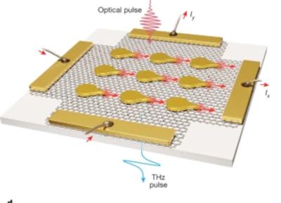
Researchers use graphene to develop new metasurface architectures for ultrafast information processing and versatile terahertz sources

Traditional microelectronic architectures are currently used to power everything from advanced computers to everyday devices. However, scientists are always on the lookout for better technologies. Recently, Los Alamos National Laboratory scientists and their collaborators from Menlo Systems and Sandia National Laboratories, have designed and fabricated asymmetric, nano-sized gold structures on an atomically thin layer of graphene. The gold structures are dubbed “nanoantennas” based on the way they capture and focus light waves, forming optical “hot spots” that excite the electrons within the graphene. Only the graphene electrons very near the hot spots are excited, with the rest of the graphene remaining much less excited.

Illustration of an optoelectronic metasurface consisting of symmetry-broken gold nanoantennas on graphene. Image from Nature

The team adopted a teardrop shape of gold nanoantennas, where the breaking of inversion symmetry defines a directionality along the structure. The hot spots are located only at the sharp tips of the nanoantennas, leading to a pathway on which the excited hot electrons flow with net directionality — a charge current, controllable and tunable at the nanometer scale by exciting different combinations of hot spots. 

Read the full story Posted: Feb 08,2024

Researchers develop self-assembling graphene sensors for modular wearable electronics

Researchers at Peking University, University of Science and Technology Beijing and Peking University Third Hospital have reported magnetically self-assembling graphene sensors. 

While wearable sensors can provide continuous, personalized health tracking beyond clinical visits, most devices today still have fixed designs targeting single applications, lacking versatility to address users' changing needs. The team's recent work could address this issue and enable modular, reconfigurable wearable electronics customized to individuals. 

Read the full story Posted: Jan 29,2024