High-speed and on-silicon-chip graphene blackbody emitters

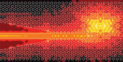
A research team from Japan has developed an integrated, high-speed and on-chip blackbody emitter based on graphene. The team reports that the device operated in NIR region including telecommunication wavelengths. A fast response time of ~ 100 ps, which is ~ 105 higher than the previous graphene emitters, has been experimentally demonstrated for single and few-layer graphene, the emission responses can be controlled by the graphene contact with the substrate depending on the number of graphene layers.

High-speed and on-silicon-chip graphene blackbody emitters image

The team stated that graphene light emitters are greatly advantageous over conventional compound semiconductor emitters because they can be integrated on silicon chips due to simple fabrication processes of graphene emitters and direct coupling with silicon waveguide through an evanescent field. Because graphene can realize high-speed, small footprint and on-Si-chip light emitters, which are still challenges for compound semiconductors, the graphene-based light emitters can open new routes to highly integrated optoelectronics and silicon photonics.
Read the full story Posted: Apr 04,2018

Japanese team synthesizes helical nanographene for the first time

Researchers from Kyoto University and Osaka University report for the successful synthesis of helical nanographene. These graphene constructs previously existed only in theory, so successful synthesis may offer applications like nanoscale induction coils and molecular springs for use in nanomechanics.

"We processed some basic chemical compounds through step-by-step reactions, such as McMurry coupling, followed by stepwise photocyclodehydrogenation and aromatization," explains first author Yusuke Nakakuki. "We then found that we had synthesized the foundational backbone of helical graphene."

Read the full story Posted: Apr 02,2018

Korean team develops a graphene-based optical modulator that mimics the human brain

The Korean state-run Electronics and Telecommunications Research Institute (ETRI) announced the development of a graphene-based optical modulator device capable of performing arithmetic and remembering it at the same time. According to ETRI, the device works much like a human brain.

The institute said its researchers have artificially recreated neural synapses in the device. It added the latest achievement will lay the foundation for the development of chips that will have a similar structure to the human brain and may also lead to the development of neuro-computers.

Read the full story Posted: Mar 05,2018

Graphene-based photonics for next-gen datacomms showcased at MWC 2018

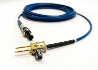
The Graphene Pavilion at the GSMA Mobile World Congress has showcased two fascinating graphene-based photonics devices. The first is said to be the world's first all-graphene optical communication link operating at a data rate of 25 Gb/s per channel, and the second one, displayed at the Ericsson stand, is the first ultra-fast graphene-based photonic switch in an Ericsson testbed. These graphene-based photonic devices may become the building blocks of the next generation of mobile networks.

All-graphene optical communication link demonstrator at MWC 2018 image

"5G will all be about optical communications, and the realization of the ultra-fast optical communication link with graphene is a real breakthrough. It is very exciting that it is already on display at the Ericsson stand," said ICREA Professor Frank Koppens from ICFO (The Institute of Photonic Sciences), Barcelona, the Scientific Chair of the Graphene Pavilion.

Read the full story Posted: Feb 28,2018

CVD Graphene prices continue to drop as commercial applications start to enter the market

CVD processes are used to create high-quality single layer (also bi-layer and tri-layer) graphene sheets. These kinds of sheets exhibit exceptional properties and can be used in a variety of exciting applications, from touch layers to transistors and sensors. For many years, CVD has been a high cost production process and this graphene is still mostly used in research projects in academic and research institutes, but prices are gradually dropping, to the point where commercial applications are starting to appear on the market.

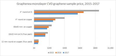
Graphenea Monolayer CVD prices (2015-2017)

Recent years have, as we said, brought on a continuing price drop in CVD graphene prices. Spain-based Graphenea, a global CVD graphene leader, has an online shop in which it offers its high-end CVD graphene samples. We have been tracking the prices of Graphenea's CVD graphene since late 2015, and the graph above shows the price decrease.

Read the full story Posted: Nov 13,2017

Graphene enables detection of single photons

A team of researchers led by the Massachusetts Institute of Technology and Raytheon BBN Technologies developed a new device that can detect single photons across a wide range of the electromagnetic spectrum, from the higher energy visible to much lower energy radio frequencies. The device consists of a sheet of graphene contacted on two ends by superconductors - a configuration called a Josephson junction.

Graphene-based single photon detector image

The ability to detect terahertz and microwave photons in this way could allow for observations of some of the faintest objects in the universe, say the researchers who report on the new technique, as well as open up new opportunities in quantum information processing.

Read the full story Posted: Sep 04,2017

Graphene enables ultra high performance infrared photodetectors

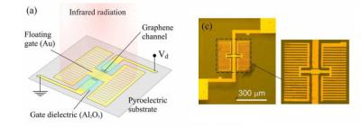
Researchers from the University of Cambridge developed a high performance room temperature graphene-based mid-infrared photodetectors. So-called "bolometers" usually feature a very low temperature coefficient of resistance (TCR) - between 2% and 4% / K.

Graphene room temperature MIR pyroelectric bolometer image

The unique properties of graphene, coupled with a novel device concept enabled the researchers to achieve ultra high performance - a TCR as high as 900%/K. The researchers hope that this device could in the future be used in astronomy, medicine imaging, automotive and even smartphone infra-red cameras.

Read the full story Posted: Aug 28,2016

Graphene and boron-nitride combine to enable efficient optoelectronics

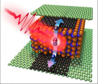
University of Washington scientists have designed a way to use graphene to encourage photons into stimulating multiple electrons, thus maximizing the transfer of energy and making efficient light-captured energetics possible.

The method exploits graphene's efficient interaction with light; The researchers took a single layer of graphene and sandwiched it between two thin layers of boron-nitride. Boron-nitride has a lattice structure very similar to graphene's, but has very different chemical properties as electrons do not flow easily within boron-nitride so it basically acts as an insulator. The team discovered that when the graphene layer's lattice is aligned with the layers of boron-nitride, a type of "superlattice" is created with desirable properties that enable efficient optoelectronics. These properties rely on quantum mechanics, and the researchers detected unique quantum regions within the superlattice known as Van Hove singularities.

Read the full story Posted: May 16,2016

Carbon Sciences enters agreement to fund project for graphene-based Cloud computing components

Carbon Sciences has been working on developing graphene-based devices for cloud computing. Now, the company announced that it has signed an agreement with the University of California, Santa Barbara (UCSB) to fund the research and development of a new graphene-based optical modulator, a critical fiber optics component needed to enable ultrafast communication in data centers for Cloud computing.

In order for data to be transmitted through a fiber optic cable, light from a laser beam must be modulated. The amount of data that can be encoded and transmitted depends on the speed of the light beam modulation. Since changing the conductivity of graphene also changes its optical properties, light passing through it will also be changed accordingly to encode digital data. This, along with graphene's impressive features are to enable the development of an ultrafast, low cost, and low power, graphene-based optical modulator.

Read the full story Posted: Dec 15,2015

Graphene and 2D crystals team up for faster optical detectors and photonic circuits

Researchers at ICFO have shown that a 2D crystal, combined with graphene, has the capability to detect optical pulses with a response faster than ten picoseconds, while maintaining a high efficiency. This can lead to faster optical detectors that can be integrated into photonic circuits.

An important advantage of these devices based on graphene (and other 2D materials) is that they can be integrated monolithically with silicon photonics enabling a new class of photonic integrated circuits. Although this study has been focused on the intrinsic properties of the photo-detection device, the next step is to develop prototype photonic circuitry and explore ways to improve large-scale production of these devices.

Read the full story Posted: Oct 06,2015