Researchers achieve nearly 90% efficiency converting light energy into surface waves on graphene

Scientists at Russia-based MIPT and Vladimir State University have reported a nearly 90% efficiency converting light energy into surface waves on graphene. They relied on a laser-like energy conversion scheme and collective resonances.
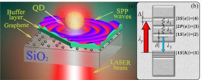
he structure for converting laser light to surface-plasmon polaritons image

Manipulating light at the nanoscale is crucial for creating ultracompact devices for optical energy conversion and storage. To localize light on such a small scale, researchers convert optical radiation into so-called surface plasmon-polaritons. These SPPs are oscillations propagating along the interface between two materials with drastically different refractive indices — specifically, a metal and a dielectric or air. Depending on the materials chosen, the degree of surface wave localization varies. It is the strongest for light localized on a material only one atomic layer thick, because such 2D materials have high refractive indices.

Read the full story Posted: Nov 17,2020

New type of graphene photodetector could enable low-cost cameras for self-driving cars and robots

An international team of researchers recently reported its success in creating a new type of graphene-based photodetector.

The team integrated three concepts to achieve the new device: metallic plasmonic antennas, ultra sub-wavelength waveguiding of light and graphene photodetection. Specifically, the 2D-material hexagonal boron nitride was used as the waveguide for hyperbolic phonon polaritons, which can highly confine and guide mid-infrared light at the nanoscale. By carefully matching the nano-antenna with the phonon polariton waveguide, they efficiently funnel incoming light into a nanoscale graphene junction. By using this approach, they were able to overcome intrinsic limitations of graphene, such as its low absorption and its small photoactive region near the junction.

Read the full story Posted: Oct 28,2020

New twist on graphene to boost optoelectronics

Researchers at University of California Berkeley, Washington University in St. Louis and Lawrence Berkeley National Laboratory have stacked two sheets of graphene on top of each other and twisted them, which resulted in the conversion of a common linear material into one with nonlinear optical capabilities. This could prove useful for various everyday technologies — from spectroscopy and material analysis to communications and computing.

In the study of optics, scientists distinguish between linear and nonlinear materials. Most materials, including sheets of graphene, are linear. If you shine red light at a sheet of graphene, the photons will either be absorbed or scattered, but in any case - they will remain red.

Read the full story Posted: Oct 21,2020

Graphene-enhanced color-changing flexible photonic crystals could be the key to next-gen smart sensors

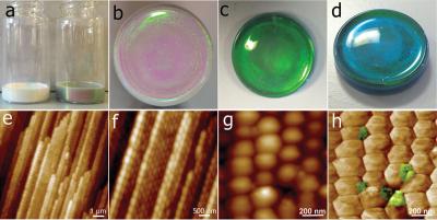
An international team of scientists, led by the Universities of Surrey and Sussex, has developed graphene-enhanced color-changing, flexible photonic crystals that could be used to develop sensors that warn when an earthquake might strike next.

Optical images and internal microstructure of graphene-enhanced colloidal crystals imageOptical images and internal microstructure of colloidal crystals enhanced with graphene. Image from Advanced Functional Materials

The wearable, robust and low-cost sensors can respond sensitively to light, temperature, strain or other physical and chemical stimuli making them an extremely promising option for cost-effective smart visual sensing applications in a range of sectors including healthcare and food safety.

Read the full story Posted: May 21,2020

A new experimental pilot line will integrate graphene and related layered materials (GRMs) in semiconductor platforms

​The European Commission recently invited a group of Graphene Flagship partners and associated members to set up an experimental pilot line to integrate graphene and related layered materials (GRMs) in semiconductor platforms.

The project aims to establish a European ecosystem covering the entire value chain, from tool manufacturers and chemical and material providers to pilot lines. This collaborative project will pioneer the manufacture of new prototype electronics, photonics and sensors integrating GRMs. The 2D Experimental Pilot Line (2D-EPL) will offer prototyping services to companies, research centers and academics to develop their innovative technologies based on 2D materials in an established processing platform.

Read the full story Posted: Apr 04,2020

Researchers develop a graphene metamaterial film that absorbs sunlight with minimal heat loss

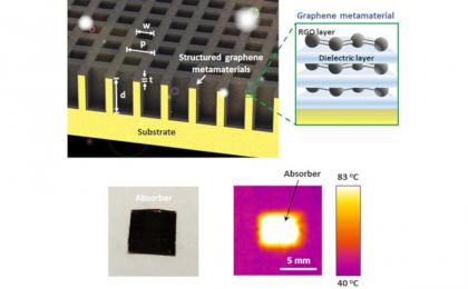
Researchers from Swinburne University developed a graphene-based highly efficient solar absorbing film that absorbs sunlight with minimal heat loss. The film rapidly heats up in an open environment and has great potential in solar thermal energy harvesting systems - in addition to other applications such as thermophotovoltaics (directly converting heat to electricity), solar seawater desalination, light emitters and photodetectors.

30nm graphene-metamaterial heat-absorbing film photo

This is the 2nd-generation material developed by the same group - now with a thickness of only 30 nm and improved performance and longer lifetime. The researchers have now created a first prototype and also suggest a scalable low-cost manufacturing process.

Read the full story Posted: Mar 15,2020

New graphene-based metasurface capable of independent amplitude and phase control of light

A KAIST research team in collaboration with the University of Wisconsin-Madison theoretically developed a graphene-based active metasurface capable of independent amplitude and phase control of mid-infrared light. This research gives a new insight into modulating the mid-infrared wavefront with high resolution by solving the problem of the independent control of light amplitude and phase, which has remained a long-standing challenge.

Light modulation technology is essential for developing future optical devices such as holography, high-resolution imaging, and optical communication systems. Liquid crystals and a microelectromechanical system (MEMS) have previously been utilized to modulate light. However, both methods suffer from significantly limited driving speeds and unit pixel sizes larger than the diffraction limit, which consequently prevent their integration into photonic systems.

Read the full story Posted: Feb 24,2020

Special substrates enable large single crystal bi-/tri-layer graphene growth

Researchers of the Center for Multidimensional Carbon Materials (CMCM) within the Institute for Basic Science (IBS, South Korea), in collaboration with UNIST and Sungkyunkwan University teams, have reported the fabrication and use of single crystal copper-nickel alloy foil substrates for the growth of large-area, single crystal bilayer and trilayer graphene films.

The growth of large area graphene films with a precisely controlled number of layers and stacking order can open new possibilities in electronics and photonics but remains a challenge. This study showed an example of the synthesis of bi- and trilayer graphene sheets larger than a centimeter, with layers piled up in a specific manner, namely AB- and ABA-stacking.

Read the full story Posted: Jan 23,2020

End-to-end processing chain of 2D materials successfully demonstrated as part of project "HEA2D"

Project "HEA2D", which started in 2016 and set out to investigate the production, qualities, and applications of 2D nanomaterials, recently demonstrated end-to-end processing chain of two-dimensional nanomaterials. The project is a collaboration between AIXTRON, AMO, Coatema, Fraunhofer and Kunststoff-Institut für die mittelständische Wirtschaft (K.I.M.W.).

It was stated that the "HEA2D" consortium successfully demonstrated an end-to-end processing chain of two-dimensional nanomaterials as part of its results. 2D materials integrated into mass production processes have the potential to create integrated and systemic product and production solutions that are socially, economically and ecologically sustainable. Application areas for the technologies developed and materials investigated in this project are mainly composite materials and coatings, highly sensitive sensors, power generation and storage, electronics, information and communication technologies as well as photonics and quantum technologies.

Read the full story Posted: Jul 23,2019

The Graphene Flagship is looking for new industrial partners for its core 3 project

The Graphene Flagship has announced a call out for new industrial partners to bring specific industrial and technology transfer competences or capabilities that complement the present GF consortium in the next core project (Core 3).

The Graphene Flagship is looking for companies with specific expertise - for example MRAM tools developers to leverage solutions for graphene-spintronic stacks, developers of graphene related materials based laser systems and instrumentations for coherent Raman imaging, makers of graphene-based fibers, yarns and textiles, automotive companies with expertise in fuel-cells, industrial graphene-based supercapacitors makers and more.

Read the full story Posted: May 09,2019