Aixtron

The Graphene Flagship details its achievements in graphene automotive technology

The Graphene Flagship, Europe's $1 billion graphene research initiative, has summed up its progress in advancing graphene-based innovations for automotive in the last ten years. The project examines, among other topics, how graphene can address key challenges in the automotive sector, such as fuel efficiency, recycling, and environmental impact.

Graphene has the potential to drive significant advancements in the automotive industry — from strengthening structural components to improving electrochemical energy storage (i.e., Batteries) efficiency and safety in electric cars as well as enhancing the performance of the self-driving car. The Graphene Flagship has orchestrated a number of projects researching the benefits of graphene in automotive applications and how vehicles can be improved. The Graphene Flagship reports it is now seeing this research and development come to fruition. Listed below are the automotive-related advancements that were achieved.

Read the full story Posted: Aug 15,2023

AIXTRON's new graphene and hBN industrial grade reactor goes into operation

AIXTRON has developed, built and installed a new, specific industrial grade reactor for graphene and hexagonal Boron Nitride (hBN) processing on 200 mm epi-wafers. The new CVD tool was developed as part of the GIMMIK research project and has recently gone into operation.

The GIMMIK project aims to evaluate the production of graphene layers under industrial conditions, spotting weak points and designing ways of eliminating the sources of error. Furthermore, the transfer of the properties of graphene to electrical components by integration into a material environment are to be tested. In parallel, methods for the large-area, contact-free characterization of graphene will be developed, which do not yet exist at present. The GIMMIK research project aims to expand graphene technology for electronic components and to bring it up to a production-relevant level. Participants of the GIMMIK project include: AIXTRON SE, Infineon Technologies, IHP GmbH - Leibniz-Institut für innovative Mikroelektronik, Protemics, LayTec, RWTH Aachen.

Read the full story Posted: Dec 22,2020

End-to-end processing chain of 2D materials successfully demonstrated as part of project "HEA2D"

Project "HEA2D", which started in 2016 and set out to investigate the production, qualities, and applications of 2D nanomaterials, recently demonstrated end-to-end processing chain of two-dimensional nanomaterials. The project is a collaboration between AIXTRON, AMO, Coatema, Fraunhofer and Kunststoff-Institut für die mittelständische Wirtschaft (K.I.M.W.).

It was stated that the "HEA2D" consortium successfully demonstrated an end-to-end processing chain of two-dimensional nanomaterials as part of its results. 2D materials integrated into mass production processes have the potential to create integrated and systemic product and production solutions that are socially, economically and ecologically sustainable. Application areas for the technologies developed and materials investigated in this project are mainly composite materials and coatings, highly sensitive sensors, power generation and storage, electronics, information and communication technologies as well as photonics and quantum technologies.

Read the full story Posted: Jul 23,2019

AIXTRON demonstrates new graphene production systems

AIXTRON recently showcased two of its systems, which enable cost effective graphene production for a myriad of applications such as consumer electronics, sensors and photonic applications.

AIXTRON exhibits graphene production systems imageAIXTRON's new 'Neutron' roll to roll system for the production of graphene. Credit: AIXTRON

Graphene Flagship partner AIXTRON introduced results from two of its systems that enable the large-scale production of graphene through chemical vapor deposition (CVD). The Neutron is a roll-to-roll system capable of depositing large areas of graphene on metal foils under ambient conditions; and the CCS 2D system enables wafer-scale production of graphene on insulating wafers, a breakthrough that could speed up the development of new graphene electronics.

Read the full story Posted: Jul 03,2019

Aixtron takes part in “HEA2D” project to investigate the production, qualities, and applications of 2D nanomaterials

Aixtron, a leading provider of deposition equipment, is working together with five partners in the “HEA2D” project to investigate the production, qualities, and applications of 2D nanomaterials.

The joint project is now researching an end-to-end processing chain consisting of various deposition processes for 2D materials, processes for transfer onto plastic foils, and mass integration into plastics components. AIXTRON’s partners for implementing systems technology and integrating materials into plastic molded parts are the Fraunhofer Institute for Production Technology (IPT), Coatema Coating Machinery, and Kunststoff-Institut Lüdenscheid (K.I.M.W.). This work is being supported in terms of nano-analytics and the development of prototype components by the Institutes of “Electronic Materials and Nanostructures” (University of Duisburg-Essen) and “Graphene-based Nanotechnology” (University of Siegen).

Read the full story Posted: Jul 25,2016

Experts roundup: will CVD ever be a viable commercial way to produce graphene?

Graphene-Info is happy to introduce a new feature: Experts Roundup. We asked several graphene professionals to answer a graphene related question. We hope this will prove to be an interesting read and can help shed light on the nooks and cranks of the graphene industry. Enjoy!

Do you think CVD will ever be a viable way to mass produce commercial graphene sheets?

Gonçalo Gonçalves, product marketing specialist, Aixtron: Chemical vapour deposition has been used for several decades in the semiconductor industry to deposit high-quality thin-films. This technique is known to provide superior process reliability and throughput which are key requirements in the manufacturing of integrated circuits. Since 2004, graphene has emerged as a wonder material with an impressive number of potential applications across several fields. The discovery of a CVD route to produce graphene has also been an important achievement towards the integration of this carbon nanomaterial into semiconductor devices. With the advance of the graphene field from basic to applied research new and more complex challenges arise, especially in the integration reliability. CVD technique will find its way to mass production of graphene once these challenges are addressed and the benefits of graphene in semiconductor devices are unveiled.

Read the full story Posted: Jul 20,2016

The Italian CNR-IMM orders an AIXTRON BM Pro system

Aixtron, a leading global provider of deposition equipment to the semiconductor industry, has announced that the Institute for Microelectronics and Microsystems of the Italian National Research Council (CNR-IMM) in Catania, Italy, has purchased a BM Pro system in a 6-inch wafer configuration.

The equipment will be used to produce carbon nanotubes and graphene for the WATER (Winning Applications of Nano Technology for Resolutive Hydropurification) project, focused on the use of nanomaterials for water purification. In particular, the research is investigating carbon nanostructures, such as nanotubes and graphene, that have turned out to be the most promising nanomaterials for such applications. 

Read the full story Posted: Feb 04,2016

European researchers reach graphene production breakthrough, under project GRAFOL

Researchers involved in the €10.6 million European research project called GRAFOL have reportedly demonstrated a cost-effective roll-to-roll production tool capable of making large sheets of graphene on an industrial scale. The tool operates at atmospheric pressure and at reduced operating temperature, and is proclaimed by the researchers "the best route to low-cost manufacture".

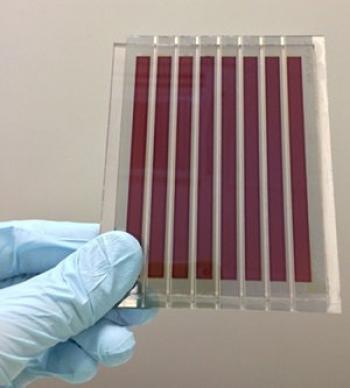
Graphene-enhanced perovskite PV

The project team also believes that graphene could be used as a substitute for transparent indium tin oxide (ITO) electrodes used in organic LEDs (OLEDs), enabling flexible designs while helping reduce dependency on ITO. In addition, the team showed that it is possible to adapt the CVD method to grow graphene on 300 mm-diameter silicon wafers the standard size currently used in the semiconductor industry. That suggests the potential to integrate graphene in silicon photonics platforms, as well as flexible thin-film solar cells with transparent electrodes (like perovskite PVs, for example).

Read the full story Posted: Dec 18,2015

A novel way to produce graphene proves green and sustainable

Researchers from DTU Nanotech and collaborators at DTU Danchip, DTU Energy, Columbia University USA and Aixtron Ltd, UK have found a greener, more sustainable way of producing graphene. Their method not only reduces the amount of copper needed for growth but also reuses the copper.

The scientists minimized the amount of copper needed for growth from 50 µm thick foils to 100 nm thick layers supported by silicon wafers. To transfer the graphene, they used a novel electrochemical method in a liquid electrolyte. This method involves oxygen from the atmosphere, dissolved in a liquid electrolyte in between the copper and graphene layer. By applying a reducing potential, the oxidised copper surface is changed back to copper without dissolving it, and at the same time releasing the graphene. This works well because graphene does not tend to stick to copper oxide and reducing the copper oxide results in a volume decrease which helps further to release the graphene from the catalyst surface.

Read the full story Posted: Apr 20,2015

Aixtron to supply a reactor to Nano Carbon (Poland)

The leading German deposition equipment provider Aixtron announced that Nano Carbon (Poland) has ordered AIXTRON’s AIX G5 WW reactor for graphene production on silicon carbide. Nano Carbon owns a low-cost patented technique for epitaxial graphene that can be implemented on the AIXTRON system.

The equipment was ordered in the first quarter of 2015 and is due for delivery by the fourth quarter. The system will be configured to handle either ten 100mm or six 150mm substrates per run. The AIX G5 WW equipment provides high wafer throughput and is designed for the ultra-high temperatures needed for epitaxial graphene on SiC deposition.

Read the full story Posted: Mar 19,2015