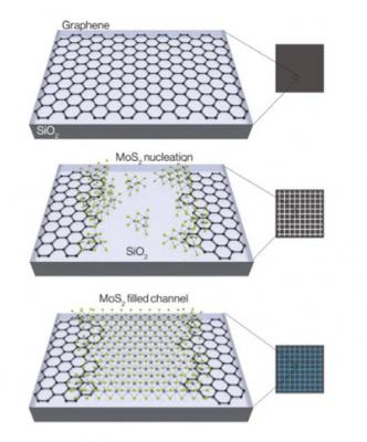
Researchers at the U.S. Department of Energy’s Lawrence Berkeley National Laboratory (Berkeley Lab) have developed a way to assemble transistors based on graphene and molybdenum disulfide.

The method etches narrow channels in conducting graphene laid down on a silicon-dioxide substrate. These channels are then filled with the 2D MoS2. The method allows graphene to inject electrons into the conduction band of the MoS2 channel with improved performance compared with simply using metal contacts to inject electrons, according to the researchers.
The synthesis method was able to cover an area a few centimeters long by a few a millimeters wide, opening up the possibility of commercial-scale production in a wafer fab on a silicon wafer. The research team assembled the transistor into the logic circuitry of an inverter underscoring its applicability to commercial IC production.
The researchers stated that "Both of these two-dimensional crystals have been synthesized in the wafer scale in a way that is compatible with current semiconductor manufacturing. By integrating our technique with other growth systems, it's possible that future computing can be done completely with atomically thin crystals".