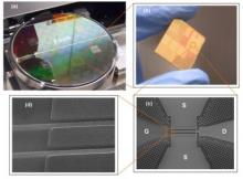
IBM researchers has fabricated a 2-GHz graphene frequency doubler RF circuit in a CMOS-compatible manufacturing process, on 8" wafers. To fabricate this the researchers inverted the usual manufacturing process and define gate structures first on silicon wafers and then transfer graphene layers fabricated using chemical vapor deposition to the silicon. After defining the areas of graphene IBM was able to attach source and drain contacts to the graphene to complete FET structures.
 Inverted-T gate structure
The device itself, the frequency doubler, integrates multiple field effect transistors and radio frequency passives and demonstrated a conversion gain of approximately -25db (at 2 Ghz).
Posted: Sep 18,2011 by Ron Mertens

