Researchers from the University of Nottingham’s Centre for Additive Manufacturing (CfAM) have reported a breakthrough in the study of 3D printing electronic devices with graphene.
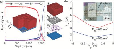
 Characterization of the fully inkjetâprinted graphene/hBN FET. Photo from article
The scientists utilized an inkjet-based 3D printing technique to deposit inks that contained flakes of graphene, in a promising step towards replacing single-layer graphene as a contact material for 2D metal semiconductors.
The scientists leveraged several advanced manufacturing techniques, including inkjet 3D printing, micro-Raman spectroscopy, thermal gravity analysis, and electrical measurements. Combined, these technologies provided the researchers with a substantial structural and functional understanding of inkjet-printed graphene polymers and the effects of heat treatment on their performance.
During the study, the researchers 3D printed inks containing tiny flakes of graphene into multiple layers, to facilitate inter-flake quantum tunneling, a process in which the electrical properties of printed layers are strongly influenced by the graphene flakes’ packing fraction, and by meandering electron trajectories which traverse the layers.
According to the laws of quantum mechanics, in which the electrons act as waves rather than particles, we found electrons in 2D materials travel along complex trajectories between multiple flakes. It appears as if the electrons hop from one flake to another like a frog hopping between overlapping lily pads on the surface of a pond, explained Fromhold.
By controlling these trajectories, the scientists were able to produce a fully inkjetâprinted field-effect transistor (FET), consisting of a graphene layer and a top gate of hexagonal boron nitride (hBN). The researchers claim this is the first time that inkjet-printed graphene has successfully replaced single-layer graphene as a contact material for 2D metal chalcogenides chemical elements also known as the oxygen family. The development has thus initiated a new wave of research into 3D printed 2D electronics for photon detectors, sensors, and capacitors, for stretchable and wearable electronics.
While 2D layers and devices have been 3D printed before, this is the first time anyone has identified how electrons move through them and demonstrated potential uses for the combined printed layers, said Lyudmila Turyanska of CfAM. Our results could lead to diverse applications for inkjet-printed graphene-polymer composites and a range of other 2D materials.
According to Turyanska, in addition to wearable electronics, the findings could aid in the production of a new generation of functional optoelectronic devices, such as large and efficient solar cells and printed computers.
The researchers will go on to explore how to better control the deposition of the graphene flakes within the ink through the use of polymers, and will test several different inks with a range of flake sizes. In this next stage, the scientists will attempt to develop more sophisticated computer simulations of the materials and how they interact, with the ultimate aim to uncover ways of mass-manufacturing the prototype devices.
The study was jointly carried out by CfAM engineers and physicists at the University of Nottingham’s School of Physics and Astronomy under a £5.85 million EPSRC-funded program grant.

