New graphene biosensor can detect SARS-CoV-2 in under a minute
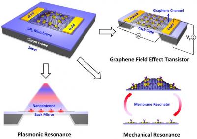
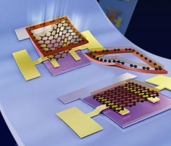
Korean researchers have developed a graphene-based field-effect transistor-based biosensor that detects SARS-CoV-2 in nasopharyngeal swabs from patients with COVID-19, in less than one minute.
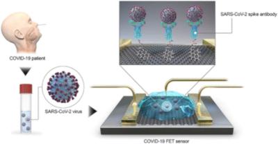
Currently, most diagnostic tests for COVID-19 rely on a technique called real-time reverse transcription-polymerase chain reaction (RT-PCR), which amplifies SARS-CoV-2 RNA from patient swabs so that tiny amounts of the virus can be detected. However, the method takes at least 3 hours, including a step to prepare the viral RNA for analysis. Edmond Changkyun Park, Seung Il Kim and colleagues wanted to develop a faster diagnostic test that could analyze patient samples directly from a tube of buffer containing the swabs, without any sample preparation steps.


