Improved graphene transfer process may boost device fabrication

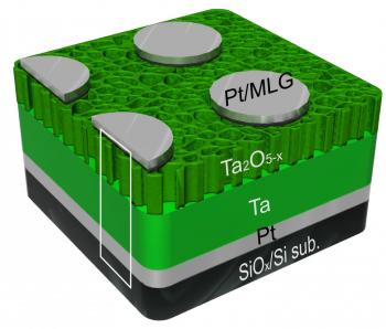
Scientists from Germany, the Netherlands, Spain and Saudi Arabia, along with Graphenea, designed an improved process for achieving wafer-scale fabrication of graphene devices. The process is said to be reliable and produce graphene sheets that are smooth and uniform across the wafer, conformally covering the electrode structures. 

The process relies on a series of actions that overturns traditional fabrication norms - lithography and contact evaporation are performed prior to graphene transfer. In the research, the scientists studied the values reported in literature for contact and sheet resistance obtained with the standard graphene fabrication and transfer method. Focusing on graphene grown by CVD, they found that there is significant scatter in the reported values. The scientists then performed the standard procedure themselves, finding that the resulting graphene sheet is inhomogeneous, with defects appearing in random places. 

Read the full story Posted: Aug 12,2015

Graphene-tantalum sandwich makes for high-density solid-state memory

Scientists at Rice University have created a solid-state memory technology based on graphene and tantalum oxide (a common insulator in electronics) that allows for high-density storage with a minimum occurrence of computer errors.

Applying voltage to a graphene, tantalum, nanoporous tantalum oxide and platinum structure creates addressable bits where the layers meet. Control voltages that shift oxygen ions and vacancies switch the bits between ones and zeroes. This design may allow for crossbar array memories that store up to 162 gigabits, higher than other oxide-based memory systems under investigation by scientists. 

Read the full story Posted: Aug 11,2015

New graphene-enhanced hockey stick to hit the market soon

Sher-Wood Hockey, maker of ice hockey equipment, is getting ready to launch their new graphene-enhanced carbon fibre Rekker EK60 stick. The Rekker EK60 is scheduled to debut on September 4th 2015, and will be made of an extremely light and strong compound that should help keep it under 400 (385, to be exact) grams and improve upon durability.

The use of graphene in this hockey stick is meant to redistribute weight and support it against impact in key breakage areas. It aims to be the most lightweight, durable and responsive stick yet.

Read the full story Posted: Aug 10,2015

CVD variant minimizes quality gaps between synthetic and natural graphene

A collaboration between Flagship-affiliated physicists from RWTH Aachen University and Forschungszentrum Jülich, together with colleagues in Japan, devised a method for peeling graphene flakes from a CVD substrate with the help of intermolecular forces. It is an innovative variant on the traditional CVD process, which yields high quality material in a scalable manner, that might significantly narrow the performance gap between synthetic and natural graphene.

The process is heavily based on the strong van der Waals interaction that exists between graphene and hexagonal boron nitride, another 2D material within which it is encapsulated. Thanks to strong van der Waals interactions between graphene and boron nitride, CVD graphene can be separated from the copper and transferred to an arbitrary substrate. The process allows for re-use of the catalyst copper foil in further growth cycles, and minimizes contamination of the graphene due to processing.

Read the full story Posted: Aug 10,2015

Lasers can be used to modify the properties of graphene

Researchers from Technological Center AIMEN explored the use of ultrafast lasers as tools for graphene processing and found that laser beams can be focused to tailor the properties of graphene films in finely defined areas to produce distinct behaviors useful for various devices. The speed of the process can be higher than one m/s for drawing the micrometer-sized features. Processing speeds over 10 m/s could be attained using advanced optical scanning.

The method is based on the use of short, highly controlled laser pulses, which induce chemical changes in the carbon lattice. A single pulse of laser with a duration of several picoseconds is enough. At this timescale, the researchers demonstrated that they can pattern graphene lattices by cutting, adding external molecules or binding compounds (functional groups like oxygen or hydroxyl). As the laser spot can be focused in an area of one square micron or less, direct writing of devices on graphene can be achieved with high precision, producing nano-devices with minimal footprint and maximum efficiency.

Read the full story Posted: Aug 09,2015

Graphene-perovskite hybrids enable ultra-efficient photodetectors

Researchers from the EPFL in Switzerland have created the first perovskite nanowire-graphene hybrid phototransistors. Even at room temperature, the devices are highly sensitive to light, making them outstanding photodetectors. 

Perovskites are known for their efficient capability of turning light into electricity, which is why they are attracting massive interest in the solar field. The scientists microengineered nanowires out of the perovskite methylammonium lead iodide, in an intricate method that was developed in 2014 and called slip-coating method. The advantage of nanowires is their consistency, while their manufacturing can be controlled to modify their architecture and explore different designs. 

Read the full story Posted: Aug 08,2015

Saab is looking at graphene for camouflage and defense applications

Saab, a global company that provides world-leading products, services and solutions from military defense to civil security, is looking at applying Graphene in signature management primarily known as detection avoidance. Graphene, in combination with other natural substances, could be used to actively change the shape and topology of all manner of surfaces, including ships, aircrafts and even military uniforms.

Read the full story Posted: Aug 08,2015

Israel-based SP Nano secures $850,000 to develop graphene-enhanced carbon fiber sizing

SP Nano, a specialist in nanotechnology for enhanced textiles and composite materials, has received $850,000 in grant funding from the US-Israel Bi-national Industrial Research & Development (BIRD) Foundation to develop a system for graphene-enhanced carbon fiber sizing with its USA based partner, Graphene Technologies.

SP Nano is the developer of SP1, a nano-reinforcement protein agent that aims to transform the composite materials and rubber industries by enabling the production of lighter, stronger and sustainable parts. SP Nano is commercializing the use of carbon-based nanoparticles in the rapidly growing $152 billion US mechanical rubber goods (MRG) and $90 billion US composites markets. These markets includes raw materials such as carbon/glass fiber and aramid, and are commonly used in industries such as aerospace, construction, automotive and marine, wind energy and sports equipment.

Read the full story Posted: Aug 06,2015

New graphene-based hybrid material may transform night vision and cameras

Northeastern University scientists were commissioned by DARPA (Defense Advanced Research Projects Agency) and ARL (Army Research Laboratory) to modify graphene to provide thermal sensitivity for use in infrared imaging devices such as night-vision goggles for the military. In a four-year project set out to do just that, they ended up creating an entirely new material spun out of boron, nitrogen, carbon, and oxygen that shows evidence of magnetic, optical, and electrical properties as well as DARPA's sought-after thermal ones.

The potential applications of such a material are varied and range from 20-megapixel arrays for cellphone cameras to photodetectors to atomically thin transistors that when multiplied by the billions could fuel computers. 

Read the full story Posted: Aug 06,2015

UK researchers working with graphene inks to develop improved batteries and supercapacitors

Researchers at Manchester Metropolitan University in the UK, funded by £500,000 from the Engineering and Physical Sciences Research Council, are striving to use graphene inks to print intricate 3D structures, in hopes to increase the charge storage of batteries and supercapacitors that they create. 

The scientists are involved in a project, meant to run about three and a half years, to create graphene-based energy storage systems. They are trying to achieve a conductive ink that blends the extraordinary properties of graphene with the ease of use of 3D printing to be manipulated into a structure that’s beneficial for batteries and supercapacitors.

Read the full story Posted: Aug 05,2015