Researchers from the University of Arizona discovered how to change the crystal structure of graphene with an electric field. This unique technique may enable graphene transistors - and electronics and microprocessors applications.
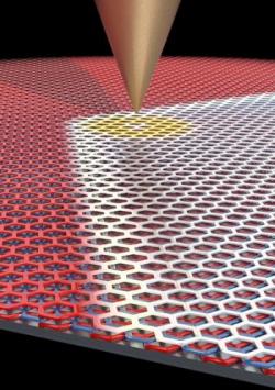
The researchers used trilayer graphene, in which the top layer can be placed in two different ways - either the atoms are placed on the atoms of the bottom layer or with a slight offset (so the atoms are placed on the space between the bottom layer atoms). In a tri-layer graphene sheet, this happens naturally and actually the two stacking configurations exist together with a sharp boundary between them.
When there's such a boundary, one side behaves as a metal, while the other side behaves as a semiconductor. Using an electric field (applied by an extremely sharp metal scanning tunneling microscopy tip) the researchers could move the position of the domain "wall". This changed the crystal structure of the trilayer graphene.
By applying an electric field to move the boundary, it is now possible for the first time to change the crystal structure of graphene in a controlled fashion - and basically change the material from metallic to semiconductor and vice versa - and this can be used to control the flow of electronics, or a basic on/off switch. The graphene could operate as both a p-type or n-type transistor.