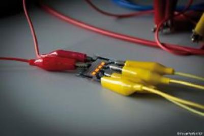
A few days ago we reported that the Fraunhofer Institute FEP will demonstrate an OLED device with a graphene-based electrode, as part of project GLADIATOR. The researchers hope that the graphene will enable devices that are highly flexible and stable. The CVD-produced monolayer graphene was produced by Graphenea, and the project that will run until April 2017 aims to produce larger demonstrators.
We had the good chance of talking to Beatrice Beyer, the project's coordinator at the Fraunhofer Institute, and she was kind enough to answer a few questions we had regarding the project and the technology they develop.
Q: Beatrice, thanks for your time. Can you explain to us how the graphene compares to ITO as an OLED electrode?
For the time being, the optoelectronic performance of graphene as a transparent electrode is still not as good as for the mature 'industry standard' ITO, but the performance and production technologies are continuously improving and we are optimistic that soon graphene based devices will reliably compete with ITO based on performance.


Q: What are the advantages of using graphene in such applications?
Once the desired optical and electrical properties on large area are achieved, the graphene electrode will surpass ITO with regard to its mechanical stability so there are very good chances that graphene will enter successfully the market in flexible electronics, which will be also still very dynamic.
Q: And what are the challenges you had to overcome on the way to this first demonstrator?
Definitely the quality. Although you can synthesize very pure and high quality graphene, it is hard to avoid introducing lots of defects during the transfer to your target substrate this is the main challenge. Once they are introduced, it is very difficult to get rid of them while keeping the performance of graphene at a high level.
Q: Any thoughts on how close is this to commercialization?
Difficult to tell. The production costs have to be reduced a lot to compete with ITO, in particular considering the high requirements for transmittance and conductivity. It also depends a bit if other application areas (e.g. for touch sensitive surfaces) will adopt graphene as an electrode - this would accelerate the scale-up and thus the approach to economically viable transparent graphene electrodes for optoelectronic devices. Commercialization will certainly occur in the near future, however the production volume can hardly be predicted.
Q: Can you explain to us why you chose graphene monolayers produced by CVD and not graphene flakes which can be made in more economic ways?
Indeed the combination of graphene with silver nanowires or mesh has also demonstrated impressive performance and we are closely observing such developments. However, besides the fact that the performance is still below our requirements (T ~ 90%, RSh ~ 10 â¦/sq.) we need a very flat electrode for thin film electronics. Since the use of metal nanowires or mesh implies a degree of topography or roughness, we are focusing our effort on doped CVD graphene to achieve the desired properties.
Thanks Beatrice, good luck in this project and I hope we'll hear more good news from you soon!