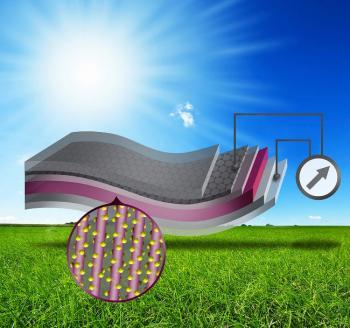
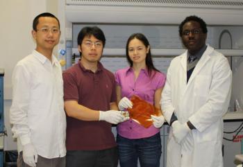
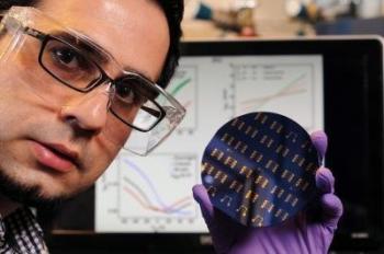
December 2012

The UK gives £21.5 million more for graphene research

The UK announced extra funding of £21.5 million ($34.7 million) to boost graphene research and development in the UK. This new investment fund aims to "take the technology from the lab to the factory floor".

The Imperial College in London will receive the largest sum (£4.5 million) to investigate aerospace applications of graphene. Other projects are based at Durham University, the University of Manchester, the University of Bath together with the University of Exeter (£1.1  million) and Royal Holloway. All of those universities will collaborate with industrial partners (including Nokia, BAE Systems, Procter & Gamble, Qinetiq, Rolls-Royce, Dyson, Sharp and Philips Research). The commercial companies will take part in the funding and will invest £12 million more.

Read the full story Posted: Dec 27,2012

MIT researchers develop a flexible graphene-based solar panel

Researchers from MIT developed a new solar (photovoltaic) cell that is made from several graphene sheets coated with nanowires. They say that this flexible and transparent cell could be made on the cheap.

The new solar panels use graphene as a replacement for ITO. The new electrode material is cheaper and provides several advantages over ITO: flexibility, low weight, mechanical strength and chemical robustness. The idea is to use a series of polymer coatings to modify the graphene properties, allowing them to bond a layer of zinc oxide nanowires to it, and then an overlay of a material that responds to light waves—either lead-sulfide quantum dots or a type of polymer called P3HT. Despite these modifications, graphene's innate properties remain intact.

Read the full story Posted: Dec 23,2012

The NanoMaster project developed new graphite materials used to produce high-quality graphene

NanoMaster project logoThe European NanoMaster project (a EC Seventh Framework funded project which started on December 2011 and is being led by NetComposites, UK, and involves 12 other project partners including Philips) has developed new grades of expanded graphite - used to produce high-quality graphene. The project aims to develop up-scale processing methods for production of graphene and expanded graphite reinforced thermoplastic masterbatches and compounds.

The new expanded graphite and nano-graphite materials are designed to be easier to exfoliate in both chemical and mechanical processes and are also useful when trying to tailor the properties of the final composite for different applications. As part of the project, high quality graphene has been produced from those new graphite materials via a multiple-stage chemical exfoliation process involving oxidative treatment, washing, filtration and reduction.

Read the full story Posted: Dec 19,2012

Zhejiang University ordered an Aixtron BM 2" R&D system for graphene and CNT research

Aixtron announced that China's Zhejiang University has ordered an AIXTRON BM 2-inch R&D system. The system (which was ordered in Q2 2012 and which will be delivered in Q4 2012) will be used for advance CNT and graphene research.

The BM R&D system features a high performance, fast response heater (1000° C/minute ramp rate) which enables complex process steps at different temperatures to be reproducibly implemented, such as catalyst pre-annealing, growth and post annealing.

Read the full story Posted: Dec 13,2012

Flexible graphene FET features record current densities, power and conversion gain

Researchers from the University of Texas at Austin have developed flexible graphene field-effect transistors (G-FET) that features record current densities and the highest power and conversion gain ever. The team says that the transistors show near symmetric electron and hole transport and are the most mechanically robust flexible graphene devices fabricated to date. They are also resistant to water.

The G-FETs were made directly atop patterned dielectrics on plastic sheets using conventional microelectronic lithography. In those devices, multi-finger metal gate electrodes are embedded in the plastic sheet. The graphene was grown using CVD.

Read the full story Posted: Dec 11,2012

P-N junctions in graphene developed using self-assembled monolayers

Researchers from Georgia Tech have developed a new low-temperature method to dope graphene films using self-assembled monolayers (SAM) that modify the interface of graphene and its support substrate. Using this method the researchers developed graphene p-n junctions.

The researchers used CVD to grow graphene on copper film and then transferred it to silicon dioxide substrates that were functionalized with the self-assembled monolayers. Thus they have shown that you can make fairly well doped p-type and n-type graphene controllably by patterning the underlying monolayer instead of modifying the graphene directly. All previous methods (such as substitution of carbon atoms for nitrogen atoms, compounds addition or graphene ribbons edge modification) or had disrupted the graphene lattice which reduced the electron mobility and the devices were not stable.

Read the full story Posted: Dec 11,2012

Angstron Materials awarded a new patent for an NGP production method

Angstron Materials have been awarded a new patent (US #8,114,373) for its next-step method that effectively exfoliates layered graphene and offers several key advantages. Using this method one can produce nano graphene platelets (NGPs) with a thickness thinner than 100nm and in many cases thinner than 10 nm or as thin as 0.34 nm to 1.02 nm.

Angstron's process does not use undesirable chemicals, time-intensive wash steps or require high exfoliation temperatures. In addition, the method does not produce contaminated waste water and its associated disposal costs.

Read the full story Posted: Dec 09,2012

NASA is developing graphene based chemical and strain nanosensors

Researchers from NASA are developing nano-sized sensors based on graphene. The potential applications are chemical sensors (detecting atmosphere atomic traces of oxygen and other elements) and strain sensors (for detecting strains in airplane wings or spacecrafts buses). The researchers are fabricating relatively large and high quality graphene using CVD and are now applying these to sensors.

The team wants to develop small, low mass and low-power chemical detectors that could measure the amount of atomic oxygen in the upper atmosphere - for its role in creating atmospheric drag (which can cause orbiting spacecraft to lose altitude prematurely and plunge to Earth). When graphene oxidizes it changes the electrical resistance - and this can be used to measure oxygen density. Graphene could also be used to measure methane, carbon monoxide and other gases.

Read the full story Posted: Dec 06,2012