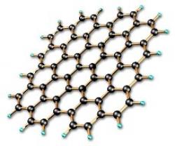
There are various methods to produce graphene materials, such as mechanical exfoliation of graphite, liquid-phase exfoliation and reduction of graphene oxide (GO), each with its own set of advantages and disadvantages. Chemical vapor deposition (CVD) is a method of producing graphene that has attracted much attention in the last decade and despite several shortcomings, is considered a leading approach to manufacture graphene, especially for applications like high-performance electronics and sensors, as it can yield high quality graphene sheets with a low defect count and good uniformity.
The CVD process
Generally speaking, the CVD method is based on gaseous reactants that are deposited on a substrate. The graphene is grown on a metallic surface like Cu, Pt or Ir, after which it can be separated from the metal and transferred to specifically-required substrates. When the gases contact the substrate inside the heated reaction chamber, a reaction occurs that creates a film of material on the substrate. The process can be simply explained as carbon-bearing gases that react at high temperatures (900-1100 °C) in the presence of a metal catalyst, which serves both as a catalyst for the decomposition of the carbon species and as a surface for the nucleation of the graphene lattice.
As was mentioned before, conditions like temperature, pressure, duration of time and many more can have a significant influence on the process and so must be carefully monitored.
Advantages and disadvantages
CVD can yield high quality graphene, with common characteristics that may include high homogeneity, imperviousness, high purity, fine grains, good control over layer number and more. However, CVD also comes with several disadvantages - namely a relatively high price of the equipment, toxic gaseous by-products and, as stated before, it is a rather sensitive process that is easily influenced by parameter changes. It is important to note that while CVD is a rather expensive method compared to other methods to produce lower-quality graphene, it is still probably the best way (to date) to acquire high quality graphene, since other ways to do that are even more expensive or complicated.


In addition, the separation (or exfoliation) of graphene from the substrate is known as challenging and it is tricky to accomplish without damaging the structure of the graphene or affecting the properties of the material. Another harrowing task is the creation of a uniform layer of graphene on a substrate, something that is continuously proving to not be easy at all.
Some approaches were and are still being developed to overcome this issue, like modifying the concentration of gases and incorporating spin coating methods, but this remains a challenge. However, despite these challenges, it is important to note that CVD is widely considered as an important and promising method to produce graphene, which is already in use, and will probably be even more so in the future, once further advancements are made. It is noteworthy that CVD is already a dominant manufacturing route for many other nanomaterials, and will assumably be in extremely common use once progress is made to resolve the issues that are currently hindering its acceptance.
Market status
While using the CVD method to produce graphene is definitely one the leading approaches in the world, it is still hindered by the challenges mentioned above. Thus, it is currently mostly limited to relatively small volumes and mainly restricted to R&D and academic uses.

However, graphene sheets produced via CVD methods are used in several applications like sensors, touch screens and heating elements. It is believed that once better answers are found to the questions of price and handling of CVD graphene, many more applications will start to appear.
Looking to buy CVD graphene sheets?
If you are interested in buying CVD graphene sheets, check out the Graphene Catalog that lists various CVD produced graphene sheets from several producers.
Researchers use graphene nanobuds as a novel anode material for lithium ion batteries
Researchers from Tecnologico Nacional de México, McGill University and Centro de Investigacion en Materiales Avanzados S.C. have examined the use of Graphene nanobuds (GNBs), formed on copper (Cu) foil via chemical vapor deposition, as an anode in lithium-ion batteries.

Producing high-performance anode materials that possess excellent specific capacities and extended cyclic ability is currently one of the key development areas in lithium-ion batteries. The energy storage capacity of lithium-ion batteries heavily depends on the anode materials used and their structure. Carbonaceous substances remain the anode materials of choice because of the strong attraction between lithium (Li) and graphitic carbon. Graphene possesses a large capacity to accommodate lithium ions in its framework because of its significant surface area and excellent electrical conductivity.
Graphene-Info updates all its graphene market report
Today we published new versions of all our graphene market reports. Graphene-Info provides comprehensive niche graphene market reports, and our reports cover everything you need to know about these niche markets. The reports are now updated to April 2022.
The Graphene Batteries Market Report:
- The advantages using graphene batteries
- The different ways graphene can be used in batteries
- Various types of graphene materials
- What's on the market today
- Detailed specifications of some graphene-enhanced anode material
- Personal contact details into most graphene developers
The report package provides a good introduction to the graphene battery - present and future. It includes a list of all graphene companies involved with batteries and gives detailed specifications of some graphene-enhanced anode materials and contact details into most graphene developers. Read more here!
Researchers design method to produce single-crystal graphene sheets on large-scale electrically insulating supports
Researchers from KAUST, Lanzhou University, Xiamen University, Friedrich Schiller University Jena and Ulsan have presented a method to produce single-crystal graphene sheets on large-scale electrically insulating supports. This approach could promote the development of next-generation nanomaterial-based devices, such as light and thin touchscreens, wearable electronics and solar cells.
Most graphene-based electronic devices require insulating supports. Yet, high-quality graphene films destined for industrial use are typically grown on a metal substrate, such as copper foil, before being transferred to an insulating support for device fabrication. This transfer step can introduce impurities that affect how well the device performs. Efforts to grow graphene on insulating supports have thus not been successful in producing the required high-quality single crystals.
Chalmers team demonstrates high charge-carrier mobility graphene through simple process
Researchers at Chalmers University have reported on a surprisingly high charge-carrier mobility of graphene.
"This finding shows that graphene transferred to cheap and flexible substrates can still have an uncompromisingly high mobility, and it paves the way for a new era of graphene nano-electronics," says Munis Khan, researcher at Chalmers University of Technology.
AGP signs a cooperation agreement with Garmor
Poland-based Advanced Graphene Products has signed a cooperation agreement with U.S-based Garmor, a division of Asbury Carbons, aiming to increase the scale of operations and expand its markets.
Advanced Graphene Products entered the Warsaw NewConnect market at the end of November last year. The company has an annual production capacity of 100kg of graphene flakes and 150m2 of single-crystal graphene sheets. This production capacity will allow commercialization of the developed graphene applications on an industrial scale.
Researchers deepen understanding of friction in graphene
A team of researchers from Korea's Pusan National University, led by Assistant Professor Songkil Kim, have examined the relationship between surface structures on chemical vapor deposition (CVD) grown graphene and its properties, specifically friction.
They correlated surface structures with nanoscale friction of a multi-layered graphene island. By cleaning the graphene surface using mechanical scratching of polymeric surface contamination, the team unveiled the surface structures such as small-scale and large-scale (folded) wrinkles on graphene using atomic force microscopy (AFM) and investigated their effect on nanoscale friction.
UK-based Paragraf raises $60 million in its latest financing round
UK-based graphene developer Paragraf has raised $60 million from the UK's Future Fund, the CIA-backed In-Q-Tel and other investors. The funds will be used to accelerate the company's device development, production and market launch.

Paragraf produces its own CVD graphene materials, which it then uses to create devices for the sensor, energy and semiconductor markets. The company introduced its first product, a graphene-based hall-effect sensor back in 2020, and it has recently concluded a study to test the deployment of graphene as an OLED electrode material.
Graphene-Info updates all its graphene market report
Today we published new versions of all our graphene market reports. Graphene-Info provides comprehensive niche graphene market reports, and our reports cover everything you need to know about these niche markets. The reports are now updated to January 2022.
The Graphene Batteries Market Report:
- The advantages using graphene batteries
- The different ways graphene can be used in batteries
- Various types of graphene materials
- What's on the market today
- Detailed specifications of some graphene-enhanced anode material
- Personal contact details into most graphene developers
The report package provides a good introduction to the graphene battery - present and future. It includes a list of all graphene companies involved with batteries and gives detailed specifications of some graphene-enhanced anode materials and contact details into most graphene developers. Read more here!
Tata Steel develops a unique few-layer rGO film material
Tata Steel has developed a new product, a few-layer film of rGO along with its collaborators at CeNS, Bengaluru. The company is now starting to mass-produce the films and offer them to application developers.
")
Figure 1: (a) Digital image of rGO/Cu foil (5 cm2). Contactact angle (b) and AFM height profile (c) on rGO/Cu
The rGO film is produced (using a modified CVD process) on copper. The film's average thickness is 5-10 nm and offers a corrosion rate of 0.02 mm/year (Tafel) and a water contact angle of ~ 97°.
These unique properties make the film suitable to protect the copper from corrosion, chemical attacks, and thermal oxidations. It also makes copper hydrophobic and can act as an antibacterial surface.
Advanced Graphene Products to go public next week at the NewConnect market
Poland-based Advanced Graphene Products S.A. (AGP), a graphene flakes and sheet developer, announced that it will go public, with a listing on the NewConnect market, on November 29th.
AGP has an annual capacity of 100Kg for graphene flakes and 150 m2 of large-area graphene sheets. The company is currently preparing to launch a pilot sale of a graphene-based filament for 3D printing.

