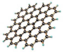
There are various methods to produce graphene materials, such as mechanical exfoliation of graphite, liquid-phase exfoliation and reduction of graphene oxide (GO), each with its own set of advantages and disadvantages. Chemical vapor deposition (CVD) is a method of producing graphene that has attracted much attention in the last decade and despite several shortcomings, is considered a leading approach to manufacture graphene, especially for applications like high-performance electronics and sensors, as it can yield high quality graphene sheets with a low defect count and good uniformity.
The CVD process
Generally speaking, the CVD method is based on gaseous reactants that are deposited on a substrate. The graphene is grown on a metallic surface like Cu, Pt or Ir, after which it can be separated from the metal and transferred to specifically-required substrates. When the gases contact the substrate inside the heated reaction chamber, a reaction occurs that creates a film of material on the substrate. The process can be simply explained as carbon-bearing gases that react at high temperatures (900â1100â°C) in the presence of a metal catalyst, which serves both as a catalyst for the decomposition of the carbon species and as a surface for the nucleation of the graphene lattice.
As was mentioned before, conditions like temperature, pressure, duration of time and many more can have a significant influence on the process and so must be carefully monitored.
Advantages and disadvantages
CVD can yield high quality graphene, with common characteristics that may include high homogeneity, imperviousness, high purity, fine grains, good control over layer number and more. However, CVD also comes with several disadvantages - namely a relatively high price of the equipment, toxic gaseous by-products and, as stated before, it is a rather sensitive process that is easily influenced by parameter changes. It is important to note that while CVD is a rather expensive method compared to other methods to produce lower-quality graphene, it is still probably the best way (to date) to acquire high quality graphene, since other ways to do that are even more expensive or complicated.
In addition, the separation (or exfoliation) of graphene from the substrate is known as challenging and it is tricky to accomplish without damaging the structure of the graphene or affecting the properties of the material. Another harrowing task is the creation of a uniform layer of graphene on a substrate, something that is continuously proving to not be easy at all.
Some approaches were and are still being developed to overcome this issue, like modifying the concentration of gases and incorporating spin coating methods, but this remains a challenge. However, despite these challenges, it is important to note that CVD is widely considered as an important and promising method to produce graphene, which is already in use, and will probably be even more so in the future, once further advancements are made. It is noteworthy that CVD is already a dominant manufacturing route for many other nanomaterials, and will assumably be in extremely common use once progress is made to resolve the issues that are currently hindering its acceptance.
Market status
While using the CVD method to produce graphene is definitely one the leading approaches in the world, it is still hindered by the challenges mentioned above. Thus, it is currently mostly limited to relatively small volumes and mainly restricted to R&D and academic uses.

However, graphene sheets produced via CVD methods are used in several applications like sensors, touch screens and heating elements. It is believed that once better answers are found to the questions of price and handling of CVD graphene, many more applications will start to appear.
Looking to buy CVD graphene sheets?
If you are interested in buying CVD graphene sheets, check out the Graphene Catalog that lists various CVD produced graphene sheets from several producers.
The latest CVD graphene news:
Navigate the emerging graphene market
This is a sponsored article by Dr Richard Collins, IDTechEx
Graphene is on the cusp of significant market growth; the opportunities are exciting and diverse, each with significant potential. Graphene and 2D Materials Europe 2020 (13-14 May, Berlin) is the largest B2B event on the topic with a dedicated focus on the commercial frontiers. www.GrapheneEurope.tech

There is often confusion surrounding the types of graphene, commercial status, and their target markets. This article will briefly summarise each and showcase what to expect at this event.
Graphene production systems maker planarTECH launches an equity crowdfunding campaign to support its future growth potential
UK-based planarTECH is launching an equity crowdfunding campaign at on Seedrs, as part of Graphene-Info's Graphene Crowdfunding Arena. planarTECH aims to expand its current business and also initiate new graphene endeavors.

planarTECH, founded in 2014, supplies CVD equipment for the production of high quality graphene sheets, as well as other 2D materials. The company was focused on research institutes, and already sold over 65 systems with a customer list that includes Manchester University, the University of Cambridge, Stanford University and the National University of Singapore.
New method uses hydrogen plasma to smooth out wrinkles in graphene
Researchers from Nanjing University in China have developed a method to make large graphene films free of any wrinkles. The ultra-smooth films could enable large-scale production of electronic devices that harness the unique physical and chemical properties of graphene and other 2D materials.
 Wrinkles in graphene films grown via chemical vapor deposition appear as jagged white lines at the top of this atomic force microscope image (left), but they disappear when the material is treated with a hydrogen plasma (right). Credit: Nature
Chemical vapor deposition (CVD) is the best-known method for making high-quality graphene sheets. It typically involves growing graphene by pumping methane gas onto copper substrates heated to temperatures around 1,000 °C, and then transferring the graphene to another surface such as silicon. But some of the graphene sticks to the copper surface, and as the graphene and copper expand and contract at different rates, wrinkles form in the graphene sheets. Such wrinkles often present hurdles for charge carriers and lower the film’s conductivity. Other researchers have tried to reduce wrinkles using low growth temperatures or special copper substrates, but the wrinkles have proven difficult to eliminate entirely, according to Libo Gao, a physicist at Nanjing University.
Graphenea launches highly flat monolayer graphene on copper thin film
Graphenea has announced the launch of a new product highly flat monolayer graphene. The graphene is grown by CVD on copper thin film on a 2 sapphire substrate. With extremely low roughness that is less than 4 nm, this new product is targeted at applications in photonics, high-performance electronics, magnetic memory, and freestanding membranes.

The product aims to meet wafer-scale integration requirements to build uniform graphene devices in a fashion compatible with current industrial fabrication methods. The flat graphene product is ready to be transferred by electrochemical delamination or dry methods since the sapphire substrate is robust enough to withstand mechanical damage, preventing tearing and wrinkling of the thin Cu sheet. The total wafer thickness is 430 micrometers. Full product information can be found in Graphenea's online store.
An activated carbon-coated lint roller can yield super-clean graphene
In order for CVD graphene to be used in its intended application, it needs to be transferred from the growth substrate to a target substrate a challenging but extremely important process step. Typically the transfer is done by spin-coating a supporting polymer layer and then chemically dissolving away the copper to release the graphene film from the substrate. The transferred graphene produced in this way is prone to contamination from the chemical agents used to remove the growth substrate as well as defective amorphous carbon generated during the high-temperature CVD growth. It also frequently leads to a substantial amount of polymer particle residue on the graphene generated during the transfer process. A third source of contamination could be airborne particles that are adsorbed onto the graphene surface.
 Top: Schematic of the activated carbon-coated lint roller for cleaning the graphene surface. Bottom left: AFM image of unclean graphene on Cu foil. Bottom right: AFM image of superclean graphene on Cu foil. Image taken from Nanowerk
Researchers from Peking University and Tsinghua University in China and University of Manchester in the UK have recently demonstrated that the amorphous carbon contaminants on CVD-produced graphene, which could greatly degrade its properties, can be removed by an activated carbon-coated lint roller, relying on the strong interactions between the amorphous carbon and activated carbon.
LG Electronics to start offering CVD graphene materials
According to our information, LG Electronics is aiming to start supplying CVD graphene materials worldwide soon, with an aim to accelerate the adoption of CVD graphene in various applications. LG is collaborating with research groups to identify new applications for graphene sheets.
![]()
LG Electronics developed its own roll-to-roll production process in addition to a specific quality control system for its graphene. LG says that its inspection system can manage uniformity deviations in crystal size, defects and electrical properties in its graphene to within 10%.
Researchers tune the CVD graphene process to achieve the longest spin lifetime ever
Researchers from ICN2 and Imec managed to demonstrate the longest spin lifetime and relaxation length ever seen in a graphene sheet.

The researchers used CVD graphene, grown on a platinum foil. By optimizing several standard processes, the researchers managed to reduce the impurity level of the graphene.
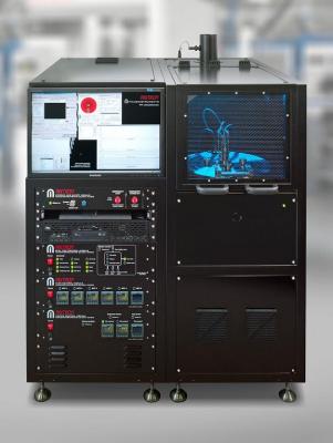
AIXTRON demonstrates new graphene production systems
AIXTRON recently showcased two of its systems, which enable cost effective graphene production for a myriad of applications such as consumer electronics, sensors and photonic applications.
 AIXTRON's new 'Neutron' roll to roll system for the production of graphene. Credit: AIXTRON
Graphene Flagship partner AIXTRON introduced results from two of its systems that enable the large-scale production of graphene through chemical vapor deposition (CVD). The Neutron is a roll-to-roll system capable of depositing large areas of graphene on metal foils under ambient conditions; and the CCS 2D system enables wafer-scale production of graphene on insulating wafers, a breakthrough that could speed up the development of new graphene electronics.
Researchers develop a graphene-based biosensor that detects bacterial presence
Researchers from Myongji University, Sungkyunkwan University, Gachon University and Korea Institute of Science and Technology in South Korea, along with U.S-based Villanova University, have developed a new device concept for bacterial sensing by Raman spectroscopy and voltage-gated monolayer graphene.

Synthesis of the monolayer graphene was done by chemical vapor deposition (CVD) on a Cu foil, which was eventually channelized onto a SiO2 /Si substrate. Modification of Raman spectra is examined in the study in order to develop ultra-sensitive biosensing techniques for the detection, identification, differentiation and classification of bacteria associated with infectious diseases.
A hands-on review of Wuxi Graphene Film's CVD graphene heating films
China-based Wuxi Graphene Film (owned by Grahope New Materials and The Sixth Element) produces patterned CVD graphene films for heating applications. These films are adopted by several Chinese device makers for different heating products - for example Grahope's graphene eye mask we recently reviewed at Graphene-Info.
The team at Wuxi Graphene Film was kind enough to send a few such films for us to review. These specific films are designed for one of WGF's customers and include a proprietary design which includes a USB connector for easy setup - you just plug these into a USB power source and the films heat up very quickly.